Looking for a new trick in LNA design.
Some feedback from the (tiny) inductance in the source grounding vias helps, (but one can have too much!)
Deliberately feeding some capacitor coupled signal from the drain to the gate via a resistor further isolated by series inductance kills the gain at low frequencies, making stability OK without badly compromising the noise figure for everywhere below about 12GHz.
Unfortunately, the setup is still unstable for frequencies above the wanted band. All kinds of messing with the feedback values seems not to do much at the high end. My stability measure is MU(load) >1
Is there some trick, or circuit arrangement, or addition, that can more affect the high frequency end to kill off the gain and bring about stability? I could use a hint here. No suggestion will be considered too outlandish.
Thanks folks ..
ATF-36077 has its charms, I know ;) Well, the tricks that made it stable are that you use not only source inductance of just right value, but also series resistor in the drain and give it also a resistive load in the gate at low frequencies.
Can you post the plot of your stability factors of the device you are using?
Sure - as soon as I can. I am temporarily travelled far away from where is the PC with all the info.
My collection of datasheets of candidate devices included ATF-36077, ATF-38143, Some Triquent Devices, and the Renesas devices from California Eastern Labs NE3210S01 and NE3511S02. The Avago devices have pretty complete data packs clearly favouring the Agilent software.
The NE3210S01 design packages (for all the famous softwares) has better complete modelling info than the NE3511S02, but is "non-promo" and not recommended for new design. The NE3511S02 has OK S-parameter data, but the symbol shows only one source connect and I had to make my own footprint layout, and I settled for file-based S-parameter only.
The layout and the vias under the sources is tricky to get right without unwanted resonances, but it needs a "just right" amount of inductance that helps lots. About the only place some resistance can be put without badly affecting noise is in series with inductance from Drain to Gate. All other matching has to be non-dissipative, or you throw away the whole point of it being an LNA.
Unstable it surely is, as are all of them. They keep that quiet in the datasheets.
While we are here on this subject, feel free to share your collection list of low noise microwave devices that are affordable, obtainable, and well characterised with good data support.
Hmm - if I thought we were all going to score a collection of great devices, maybe I was mistaken.
I do admit that the choice of good low-noise microwave devices could not honestly be described as "plentiful".
the input/output dc blocking caps want to be very small value. that way they look like open circuits at low frequency, and you at least have a standardized source/load impedance to make the thing stable with.
The via holes are really important....you want lots of them with no line length to the device.
I would use a very small package without leads!
Thanks for the reply biff44.
I do agree about the dc blocking capacitors, with the exception of the one in the drain-to-gate feedback route. That one kills the gain and brings about stability at all the lower frequencies down to DC.
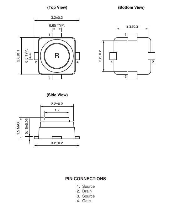
The package connections, in this model, have already have been changed from traditional 4 long leads to minimal flush tabs under for solder bump reflow, though they do protrude approx 0.5mm.
For through the last decade and more, commercial LNA's used in home satellite TV dish setups have managed to use packaged devices up to about 12GHz, though I suspect the device gain would often have been falling off above that frequency anyway.
Regarding the vias (in source inductances), simply crowding in lots of vias, or using the published test layout did not work. I had to come up with via layout shapes where the inductance could be controlled without unwanted resonances, so delivering a "just right" amount of degenerative feedback.
How much does the drain-to-gate feedback increase the NF? What is your first problem anyway, is it instability? Why don't you post your schematic and we can suggest you some solutions? What is your expected performance (G, NF @f)?
Yes - before I can get into other matchings, this is all about stability. Thus the schematic has not been determined yet. The device alone, set between S-Parameter ports, is stable (MU>1) only from about 7GHz thru 12GHz. For below, and also above the wanted 8.5GHz, it is just unstable.
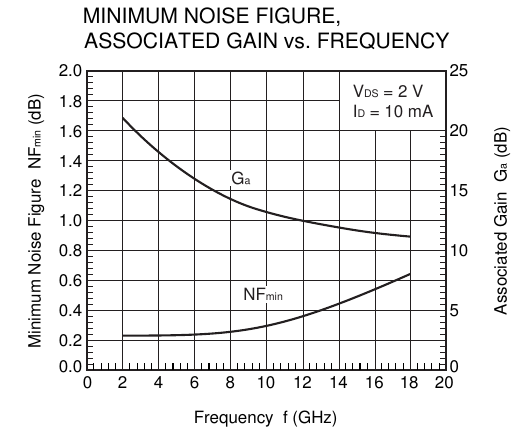
The device gain is around 20dB at 2GHz falling to about 12dB at 18GHz.
The drain-to-gate feedback I tried has capacitor + resistor+inductor in series. The final inductor physical form can be tried later. The capacitor needs to be 40pF minimum to bring stability at the very low frequencies below 2GHz. The resistor+ inductor needed to be about 900 Ohms with around 3nH to get stability from DC to about 12GHz. The region above 12GHz remains unstable.
The effect on noise figure .. the price for having a resistor in the network, is not too bad. It seems not to degrade things much provided it is behind the inductor. Any resistors anywhere in the other input matching try-outs is just catastrophic for noise.
The NFmin of this device is around 0.3dB. The stage NF rises to about 0.4dB with the feedback applied. The available gain at the wanted X-Band frequency is about 14.5dB. By the time the all the circuit is together, the NF will have slipped some more.
The final circuit will have some input matching to get to the best noise figure with acceptable VSWR mismatch - the classic trade-off. There will be inter-stage matching to a second device, and output matching up to a bandpass filter. The bias routes also have to be added.
You can do just so much with this feedback. What I need is some further circuit trick, or clever network to throw away the unwanted higher frequency gain, and get the stage stable.
Why are you forcing a resistive feedback, when you still have instability above 12GHz? When I was playing with ATF-36077, it was selfoscillating somewhere between 20 and 25GHz. Remember to check (measure, not simulate) for oscillations well above your frequency of interest with short, open, load and also a high-q device (like narrowband filter) at the LNA input. The NE devices might be more stable than that nasty ATF. Otherwise, I've mentioned already, what did the trick for me.
BTW: your RLC feedback network might become a resonant circuit at 12GHz+. Did you consider parasitics of all three at 8GHz+?
Firstly rfmw, my sincere thanks for sharing your expertise on LNA design. There are not many who do discuss this stuff. Maybe the planet is short of such folk.
Because of inexperience and ignorance while in a steep learning curve
Given the expense of constucting multiple tryout circuits on 20mil Er=3.5 substrate, with all the measurement investment (in people's time as well as hardware), I have resorted to simulation to at least get the first try somewhere near right.
I read of a "stability" example which had the CRL drain-gate feedback route. It had similar series LRC shunting both gate and drain, and user could vary or delete at will. I deleted the shunt RLC components because they would be real bad for noise. My own microstrip matching sections (no resisters!) do quite fine here. I had to learn that you fool yourself figuring stability from only S11 and S22 in a multi-stage design without checking if values visit unstable regions between the stages.
With sources grounded with lots of close vias, the device alone has load stability (mu) as in first picture..
The second picture shows the RLC feedback applied drain to gate, getting it stable down to (DC?) while keeping NFmin low.
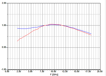
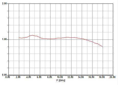
This leaves only the high frequency end still needing attention. I am happy do dump this idea entirely if I am doing something silly!
The final build would not have any lumped components near the device. The approaches for bias, etc. are with thin high inductance quarter wave decoupled lines that look like open circuit in the wanted band.
ATF-36077 was widely explored by researchers looking for "ET" and by radio amateurs. It may be urban myth, but I read that the "77" was because of a 77GHz internal oscillation :) that could be very hard to find when it happened. I think it unlikely! ATF-35143 and ATF-38143 are for 0.45-10GHz, not as wild as ATF-36077, and are in my "interesting" box.
The S-Parameter data is available for 2GHz thru 18Ghz. The non-linear model is EEHEMT, which (sort of) agrees with the measured data. That would be the only way to check outside of the range. I was hoping to find a stable way to knobble the stage gain outside of the wanted band.
I was listening, and I think I have it covered. Even with close-up clusters of vias at the sources, the gaps and widths can have unwanted resonances. I gave this a lot of attention.
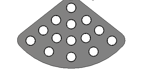
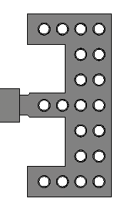
We get as close as we can without putting a via right under the foot (bad for solder!). 2 source connects makes it look like it has wings. The radial one works better.
Its OK - the damping is high, and it ceases to work other than at lower frequencies. This is a special combination where the approach to the gate is with thin high inductance line, from a lumped inductance in series. The capacitor is at the drain, with the resistor in between. It only slightly affects NFmin.
I never before thought that the device could fry itself at audio frequencies if it got going!
Small value coupling capacitors may limit the low frequency stuff from making it through, but one still has to make it stage itself safe from oscillating.
If this (feedback) is not too clever, then I would try something else. Unfortunately, just about every book / PDF I have read about making stages stable seem to use feedback and matching networks with noisy resistors in them, and especially, components in the source-ground route.
ATF-36077 is easy to be unstable and is easily burned, I prefer Japan FET to Avago.
I prefer Excelice`s FETS and NEC`s they are good.
Thanks for the reply Bob60.
I tried to Google "Excelice" and "Excelice FET", and I got a pages of stuff from ice cream to snow clearing machines.
If you maybe saved the URL of their product website, we would be pleased to check them out.
When I tried Google with "Japan FET", in similar fashion to the pointer from Bob60, I got pages of unrelated things.
Did you maybe mean "FETs from Japanese Manufacturers" ?
I already looked hard in Toshiba and NEC.
One Avago FET ATF36077 did expire unexpectedly from square-wave oscillating at audio frequency while possibly also taking some RF. Another seemed to be taking power and getting warm, maybe oscillating, but at a unknown higher frequency.
I was (sort of) hoping that this thread would eventually collect a whole bunch of favourite devices listed.
You are welcome. URL and company are dead ? but products sell successfully. Is it new selling strategy I don`t know.
http://www.rf-microwave.com/eng/cata...PA018A-70.html
same EPA025, 040, 060, 080, 120, 240
Good products doesn't needs advertisement.
Excelis had a very good product line but they closed up a year or two ago. I've not herd that anyone picked up their product line.
Ehh.. ! The PRICE! OK - if no longer made, the remaining ones will be somewhat more expensive.
BUT..
Is that a mis-print or something? 9200.00? for one, or ?8600.00 each for >10.
Rare antiques are also out of production, but maybe better value!
Anyways, if no longer made ... that is a deal-breaker.
I know I has worked a lot with these line. Problem with NEC s is limitation of the input pow~ 0dBm. It is not nice.
As for EPA that is above 10-15dBm. That`s nice. And EPA018 operate up to 30GHz with P1~ 15dBm EPA025 still work at 22-23GHz, EPA080 up to 15GHz, EPA120 up to 10GHz with P1 ~28-29dBm and so on. If you need hundreds, you can still find them. that is your interpretation, for Italian mafia ?8,600 it means eight EUR.
Of course British pound is nice and most expensive currency.
