Conductor intruding into multiple dielectric layers in ADS
I thought of a couple of things, would the solution be valid if I use vias to draw conductor lines? or, is there a way to calculate the average permittivity of the layers that this conductor pass through? (there are some other layers for other conductors)
You have to use Vias to connect these connector.
Sorry, but could you elaborate more?
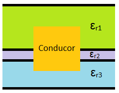
I have one horizontal conductor with a cross section that lies in different dielectrics. I cannot draw define a conductor as such in the ADS.

Like this..
You need to refine the modeling on dielectrics.
let say top dielectric is 30 mil and you have conductor passing 15 mil thick then better make two dielectric materials, bottom one with via and top dielectric matrial having no via.
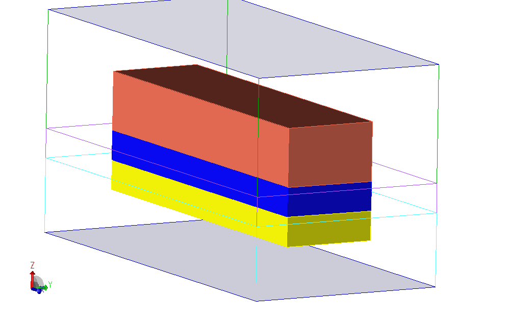
like this approximation, though momentum is 2.5D but can be made more use of 3D modeling.
Using this method, I did modeling of two PCB substrates sandwich with sphere balls.
I simulated the signal flow from bottom pcb to top PCB through this ball bonding structure.
Regards
With 3 different dielectrics you need to define and map layers to each separately so you will need 3 copies of each shape.
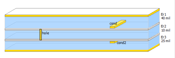
Map one layer as a thick conductor strip intruded above the interface up into the Er1 substrate. The second as a via through Er2 substrate. Finally the third would be another thick conductor strip intruded below the interface down into the Er3 sunbstrate. It would look something like this:
If the requirement is to connect top and bottom layers of Er2 then I agree with RealAEL.
but let assume the requirement is to connect dielectric loaded wave guide then model needs min 5 layers in my view.
Regards,
thnx all for the help!
I will try it RealAEL's way. I was concerned that ADS would treat vias different from conductors (vias allow only vertical currents maybe?)
multiple intruding Conductor 相关文章:
- Pairing multiple BT/BLE devices to a QCA6174A module
- Active FET mixer with multiple RF input channels, how to avoid DC blocks?
- Using multiple MLIN components on ADS
- transition length should be a multiple of a quarter of a wavelength
- Multiple Access Techniqies
- NF Measurement of Assembly with Multiple Frequency Conversions