Can this be an impedance-controlled transmission line?
I believe the differential impedances should all be 90 ohms. Is that even possible with this type of layout? It is a 2-layer PCB but there are no ground planes and there are other signals on the bottom layer.
I greatly appreciate any help!
Signal carrying traces are floating and they are neither microstipline nor coplanar waveguide since the GND isn't existing.
They should be considered Symmetrical Transmission Lines or Slotlines therefore it's possible to realize 90 Ohm Zo even it's hard...
But even each transmission line is independently realized with 90 Ohm Zo, there should be couplings between the lines and this will impact result Zo which has been desgined before.That's why, this sytem should be realized by an EM simulator otherwise the results will be very inconsistent.
I agree, differential pairs only use series inductance, and capacitance between the two wire pairs to compute the impedance.
That said, on a PCB you form a "differential pair" but just running two traces close to each other. There is nothing to stop signals on one from coupling to another differential pair on another layer. do NOT run any of the differential pairs in parallel with each other for any long length!
Also, the ground plane top and bottom might have a loading effect on the differential pairs closest to them. You would need to calculate that effect, and maybe spread out the conductors a little.
Thanks for the responses. I just wanted to clarify the image I attached. Those are all signals on the top layer of copper, not planes. There actually isn't a ground plane in the design. I have been digging into some specs related to MIPI and there are a lot of general design suggestions that were not used in this design.
How does the spacing from the return paths effect the differential impedance? Does it not effect it?
The most importance electrical property of a differential pair is the impedance the differential signal sees, which is called ‘Differential Impedance’. Since signal traveling in opposite
direction, the differential signal swing (Vdiff) is twice the voltage on either line, i.e. 2 x Vodd:
Vdiff= 2xVodd

By the definition of impedance, the impedance the differential signal sees is:
Zdiff = Vdiff/Idiff = (2xVodd)/Iodd = 2xZodd
As expressed in the formulas above, the differential impedance is twice the characteristic impedance (or odd mode impedance, Zodd) of either line. Reversely, odd mode voltage (Vodd) consumes only a half of actual voltage (Vdiff). Reducing the electric potential allows a shorter Tr / Tf so the operating frequency can be increased so more data transmitting is possible.
What do you mean with return path? Differential pairs have no return path by nature.
There are however some points to consider:
- the differential pair impndance can't be determined without considering the substrate thickness and copper on the adjacent layer. If it's mostly populated by ground, supply and slow signals, it can be probably treated as a ground plane impedance wise
- the impedance will be surely affected by the too low spacing of neighbour differential pairs
- there will be a strong coupling that questions the advantage of differential signalling
Besides a systematic calculation of differential pair impedances, your design rules should include an isolation distance between differential pairs.
Strictly spoken, the term "impedance control" involves test structures and a measurement of actual impedances in production, in contrast to "designed impedances".
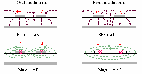
There are two types of Differential Pairs – ODD mode and EVEN mode. ODD mode is more commonly used.

- Signals have return path on adjacent layer.
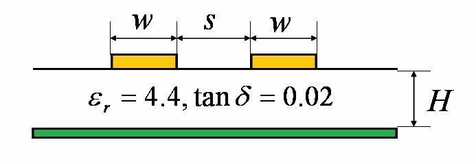
- Impedance of differential signal depends on: height of substrate, width and thickness of trace, spacing between traces.

- Impedance also depends on routing topology- microstrip & stripline.
Even and odd mode aren't "different types" of differential transmission lines, they are different wave modes of the same line.
We can safely assume, that the regular signal transmission of differential pairs is using the odd (or differential) mode. Even (or common) mode waves are either unwanted interferences or generated by non-ideal circuits and transmission line asymmetries.
In odd mode excitation of the transmission lines, currents in both lines are summing to zero, in so far there's no return path.
下一篇:difference between wave port and lumped port in HFSS
impedance controlled transmission 相关文章:
- Output Impedance Of a Triple cascode
- How to make image impedance equal
- Input and output impedance matching in Distributed amplifier
- Characteristic impedance of combination of CPWG and stripline on inner layers
- Problem of impedance matching of Gilbert cell mixer
- Input impedance of transmission lines connected in cascade
