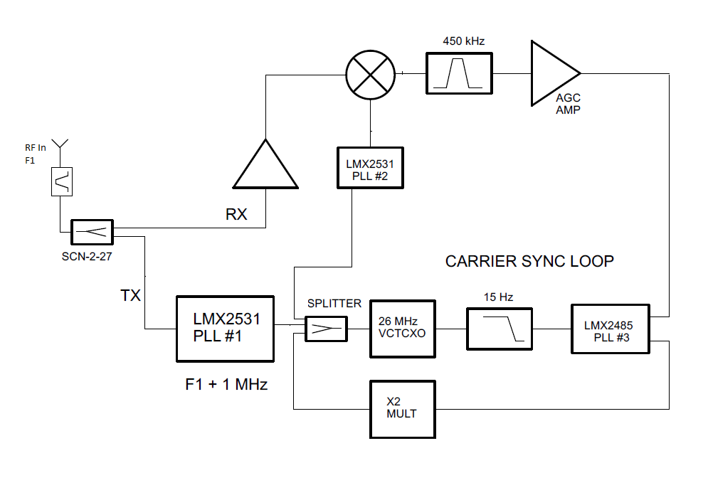
Unmodulated Carrier Recovery Circuit
The primary issue is that PLL#3 does not lock continuously. This PLL will intermittently lock and is displayed by the lock detect indicator pulsing on and off.
The general operation is: an unmodulated carrier is transmitted by another device and received at the antenna and designated F1. This signal is then down mixed to approx. 450 KHz. The 450 KHz signal is used as the oscillator input on PLL#3. PLL#3 controls a VCTCXO which is used to provide the appropriate reference clock for PLL/VCO#2.
In order to achieve the initial lock we are working on the premise that the VCTXO will be at a max or min frequency limit when PLL#3 is not locked due to the tuning output being railed high or low. The objective is to lock the VCTCXO to the device that transmits the unmodulated carriers TCXO.

Can anyone confirm the general theory/operation of this design is correct?
Thanks
I'm having trouble seeing how this thing could converge to a stable frequency... if PLL #2 outputs frequency F2, then that means the PFD to PLL #3 will be F1-F2. And the output of PLL #3's VCO must be F3=(F1-F2)/2. Thus if PLL #2 has no multiplication, then it goes that F2=F3 and F2=(F1-F2)/2, and thus F1=3F2... is that correct?
But look at the how a perturbation propagates around this loop. Let's say the output of PLL#3 is perturbed a bit high, so F3 increases a bit. PLL #2 will follow, and F2 will increase. But after the mixer, F1-F2 will decrease. That will be fed to the reference of PLL#2, which cause its output to rise still more. So in this case you get positive feedback. But if, instead, F2 happens to be greater than F1, then the loop dynamics reverse, and you might get a stable feedback....
Also feeding PLL#1 back into the antenna is problematic in itself, given that the isolation of the splitter/combiner will not be perfect.
