ATF54143 transistor layout generation problem using ADS2011.10
I want to generate the layout for ATF54143 transistor along with two MLIN's using Advanced design System 2011.10(ADS2011.10).
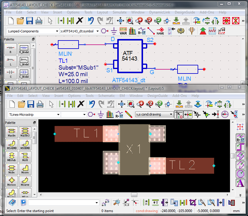
Now I generated the layout for ATF54143 transistor along with two MLIN's , have got layout generation, but it is not matching the schematic with ATF54143 and two MLIN,s. When I tried to generate the ATF54143 with two MLIN's, twice same ATF54143 transistor layout is generating in the layout view.
My question is, how to generate the proper layout generation for ATF54143 transistor and two MLIN's and also how to avoid the twice generation of same transistor layout in the layout view.
Related screen shots are attached.
Sir,
Earlier I generated the layout for ATF54143 transistor with four pins connected MLIN's using ADS2009.Layout was generated nicely without any strange appearance, but when I used ADS2011.10 and generated layout, it is giving so much trouble, I don't know why,same software with upgraded version I used.
Someone can have look on posting #1 problem and try to help me resolve layout generation problem.
It looks like you have many more elements than just the transistor.
Is cell ATF54143 in your schematic a subcircuit, with transistor model and other elements?
Then, you must assign the SMD artwork to subcircuit cell ATF54143 (and not to the transistor model in the ATF54143 subcircuit).
The model file which you have downloaded from www.avagotech.com is an old style archived project file and it does not have a package information.It consists of equivalent sub-circuit of this transistor with parasitc components.
So, you cannot create a layout with this project file.
Sir,
Tell me the remedy for this difficulty, I need ATF54143 nonlinear device model for my work.Now what I have to do, how to create proper layout for ATF54143 transistor with MLIN's using ADS2011.10. Can guide it.
This is the case that I was thinking of. The solution is simple then: assign the SOT343 layout (included with ADS) to the subcircuit cell.
Sir,
As you told, I assigned SOT343 layout also, I am not getting proper layout shape, when I generated the layout. Now also there is twice appearance of ATF54143 layout with improper shape as like earlier.
Screen shots are showed the generated and assigning SOT343 layout.
You should create a symbol view that covers all these sub-components then you have to assign a package to this top level component.
You're trying to assign a layout for the subcircuit therefore it creates nonsense layout for each..It's wrong..
You are adding the artwork to the wrong components. It gets added only to the selected component in the current schematic and not the entire schematic. Your most recent post clearly shows that you are adding the SOT343 artwork to the transmission line element TL23, it is the only item selected, inside the design ATF54143_dt.
Go to the schematic from you original post and select only the symbol for the ATF54143_dt device only and modify the artwork for that component and regenerate the layout there.
RealAEL Sir,
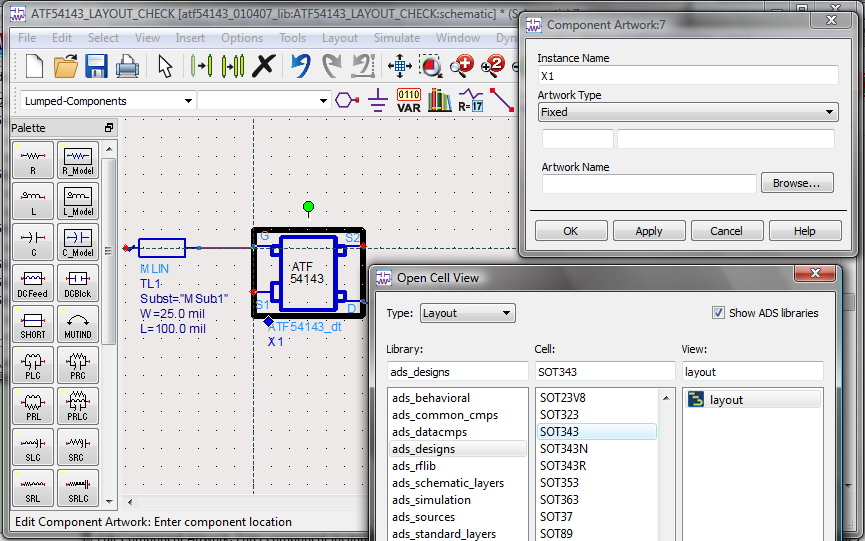
As you said, I went to schematic and selected the symbol for the ATF54143_dt device only and try to modify the artwork. But there if I browse Artwork type, it is showing only Default, it is not showing other options like fixed, null network......etc and also Artwork name Browse is not enabled to select the SOT343. This is the problem , I am facing from the beginning.
When we choose symbol ATF54143_dt from the schematic, if it shows other options such as fixed, null network and also enabled Artwork name Browse. I can easily get the generation of ATF54143 transistor symbol layout.
How to get other options such as fixed, null n/w....etc and also enabling of Artwork name to browse and select the SOT343.
Screen shot is showed the Artwork type Default and Artwork name Browse disabled.
It works perfectly for me.

Check the views for the ATF54143_dt cell. Does it have a layout view? If so delete that layout view (the whole view and not just the contents of the layout view, right click on the layout view entry in the main window and select Delete) and try again.
Have you ever tried to create a layout with this one ?It does not work because when I intend to create a layout, ADS takes sub-circuit elements instead of package component.And the layout looks like coonected some non-existing components and connections.There is definitely a trick to be considered..
RealAEL Sir,
As you said, I deleted the layout view in the main window. Now I am able to get the fixed in the artwork type and the SOT343 in the artwork name. But when I generated layout for the schematic of ATF54143 with two MLIN's, it is generating improper appearance in the layout view as like earlier twice appearance of ATF54143 transistor layout.
How to get the proper layout generation of ATF54143 transistor with four pins connected MLIN's.
It definitely can work, done it many times.

This is the old way that ADS has used to do this for many years. There is a new way available now in ADS 2011.01 and later.
Create a new empty layout view in the ATF54143_dt cell. In that view select the File > Design Parameters... then in that new UI open the third tab labelled View-Specific Configuration. Select Artwork Type Referenced/Fixed and then in the Name field enter the value ads_designs:SOT343:layout. Unfortunately there is no Browse function in this UI. Select OK to exit the UI, save the layout design even though it is still empty and the close this layout window.
In the exiting schematic view you are using it is probably best to delete the existing device symbol and place a new version. This schematic should now create the layout required.
RealAEL Sir,
As you said, I followed it and obtained the desired layout view with misplaced pin number. I have connected the MLIN's at the pin1 and pin3 in the schematic, but in the generated layout , MLIN's are attaching to the pin2 and pin3.
Pin numbers are misplacing in the generated layout view, how to assign pin numbers properly and generate the layout ATF54143 with MLIN's properly.
I have tried in my way,could obtain it.In the layout view, right click on the ATF54143 layout view and selected the open instance view and assigned the pin numbers properly,while saving I was getting problem.
In ADS2009, I have clicked on the layout view of ATF54143transistor and pushed into hierarchical view and changed the pin number very easily. In ADS2011.10, the same way I tried,I couldn't succeed it. Why same software with higher version is totally different.
The SOT layout is coming from a Read-Only library so you will not be able to directly edit it. If that becomes necessary then you would need to open the SOT343 layout view and make a copy into the current library using File > Save As... You do not need to rename the cell or the view but make sure it is saved into the current library in the workspace. You should then be able to open and edit that view and after that you would need to go back to the ATF54143_dt cell and redirect the fixed artwork name to the new SOT343 layout view in the current library rather than the original in ads_designs library.
RealAEL Sir,
Now everything is working fine, thanks for your help, you got reached me till the end of the bank of the river.
RealAEL Sir,
I am facing once again problem of generating ATF54143 layout symbol generation using ADS2011.10.
What happend you know. I followed upto what said above, I went to File > Design Parameters and selected the Fixed and enter the name ads_design:SOT343:layout and clicked O.K and exited.
Later, what I have done is deleted the existing device symbol. I wanted to place a new version symbol. But I don't know, how to place a new version of symbol.
Now I have created new schematic and try to drag the ATF54143_dt from the library, but only text of ATF54143_dt is coming, symbol is not coming and also showing error.
Now my question is, how to place a new version symbol of ATF54143_dt in the main window and getting appear of symbol ATF54143_dt in the schematic window.
layout transistor generation 相关文章:
