Finding G,S,and D of pHEMT transistor S-parameter file attach to Data Item in ADS
In the ADS, pHEMT ATF54143 transistor linear model is not available, hence I have taken the S-parameter file from the Avago technology and I have taken the DATA ITEM from the ADS component palette.The S2P data item drag and place it on the schematic and shown the path of S-parameter file of ATF54143 transistor to S2P data item.
Now I am in confusion, how to find out the Gate (G),Source(S),and Drain(D) of the pHEMT transistor S2P Data item.
Which is gate,source,and drain in the S2P Data item, when data item is attached ATF54143 transistor S-parameter file.
Can you clarify it.
Usually it must be noted in s2p file or page you downloaded it from. For example, NEC fet transistor s2p file says it measured in common source configuration, ids = ..., vds = .... So it means that S21 is between gate and drain, and source is grounded. And also i saw some formulas in internet how to convert s2p parameters from common source configuration to common gate configuration (professionals correct me if i am wrong)
Also you can refer to datasheet. Look if datasheet parameters are equal to your S2P file, then datasheet can have not on configuration (common gate, common source,...)
Sir,
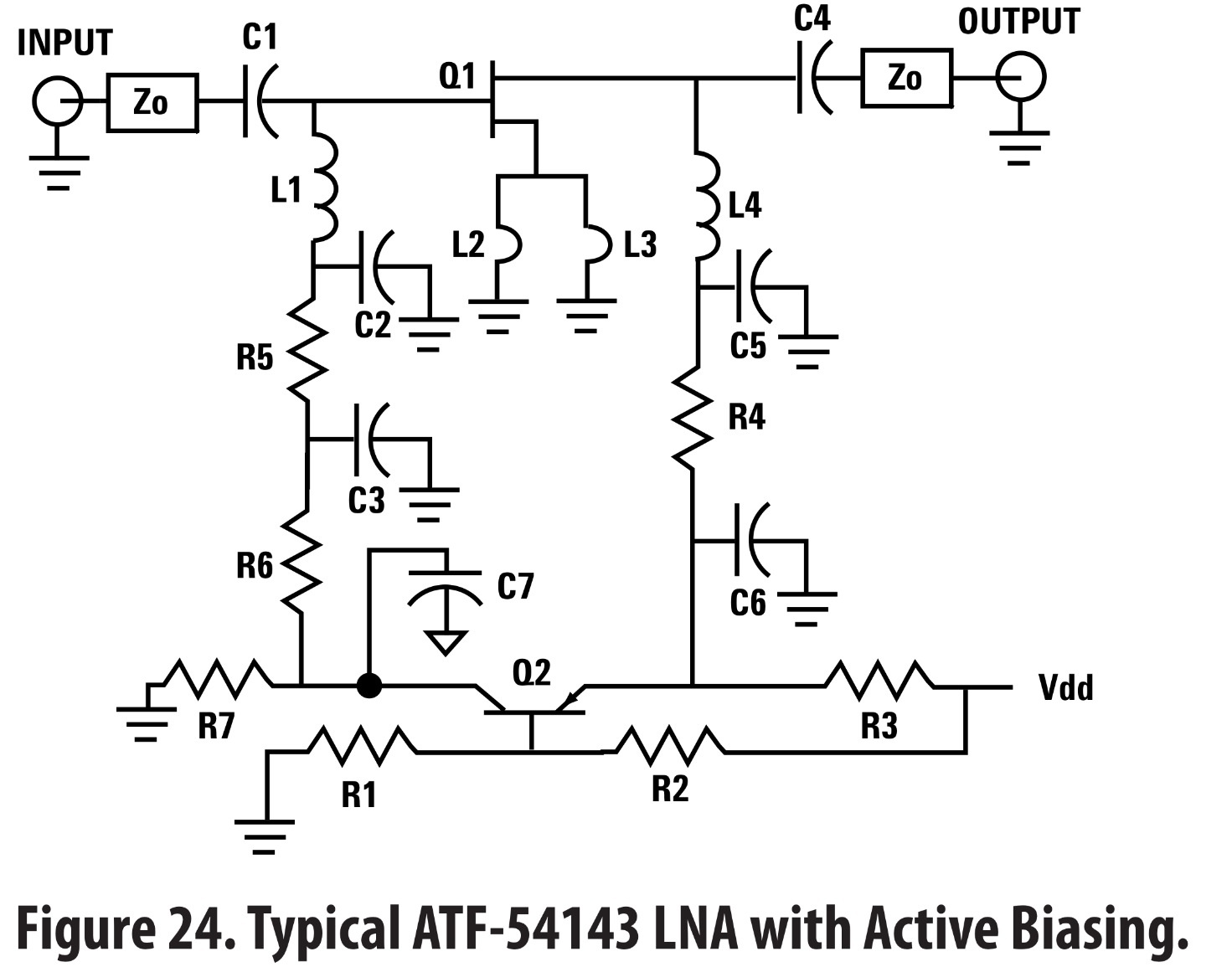
Data sheet of ATF54143, it is not mentioned, which is gate,drain,and source for linear transistor model. But in the same datasheet, nonlinear ATF54143 model has been given, there they have showed which is gate , drain , and source.
I am in confusion, how to identify the gate, drain , and source of ATF54143 transistor linear model,when S2P file is attached to the ADS data item S2P format.
Sir,
In the Avago ATF54143 datasheet, linear model of ATF54143 transistor gate, drain, and source is not mentioned. But the nonlinear model of ATF54143 transistor, it has been mentioned that which is gate,drain,and source.
How to identify the gate,drain,and source of ATF54143 transistor for linear model, when S2P file is attached to S2P of Data item of ADS. Can you someone clarify it.
Port1=Gate
Port2=Drain
Source=Grounded...
Always....
In the linear model with bias, for Sxy
Gate=Input , S1y
Drain=Output, S2y
Source=Ground ATF54143via L2,L3 on separate pads to reduce inductance.

Sir,
How we can say, port1 is gate, port2 is drain, and Source is ground. Can you justify it. Is it applicable for all FETs or is it only applicable for pHEMT.
One more question , I have, what about BJT (E,B,C) linear model S-parameters attached to the ADS data item. Can you clarify it.How we can identify BJT emitter , base , and collector in a Data item of S2P of ADS.
By International convention, schematics flow from inputs on left to outputs on right and thus S parameters are first assigned to input as Port 1.
The ground node depends on the design of a transistor configuration such as common drain, source or gate, similarly for BJT's CC, CE, CB.
The remaining node must be the Output , Port 2 by convention.
In this case, the chip is Common Source, therefore... Port 2 = Drain ... Always...
There may be inconsistency in a passive 2 port device or even a 3 port device, such as a splitter/combiner/directional coupler, which is birdirectional. When in doubt, refer to leaders in commercial test methods.
S-parameters are always measured in CE or CS configuration unless there isn't any particular remark.This is so because most conventional configuration is CE or CS.
transistor parameter Finding 相关文章:
- Cree??s CGH40010F transistor
- How to include RF Transistor Vendor Kit in Advanced Designed Design(ADS)
- Which transistor need to be chosen for designing KU-Band LNA Design high gain, low NF
- Design of LNA using CMOS transistor
- Can you help me get S-parameter file of HJFET transistor
- what type of biasing configuration is this transistor using?
