Using Load Pull analysis in ADS to design power amplifiers
I want to design a PA by Load Pull analysis in ADS at 2.95 GHz. According to its examples and the ADS's cookbook I did it, but there are some problems.
According to load pull in ADS (the below figure) if I adjust zin=250+j*1360 and zload=4.5-j15.32 I wil get PAE 64% and Pload= 44dBm.
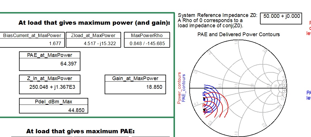
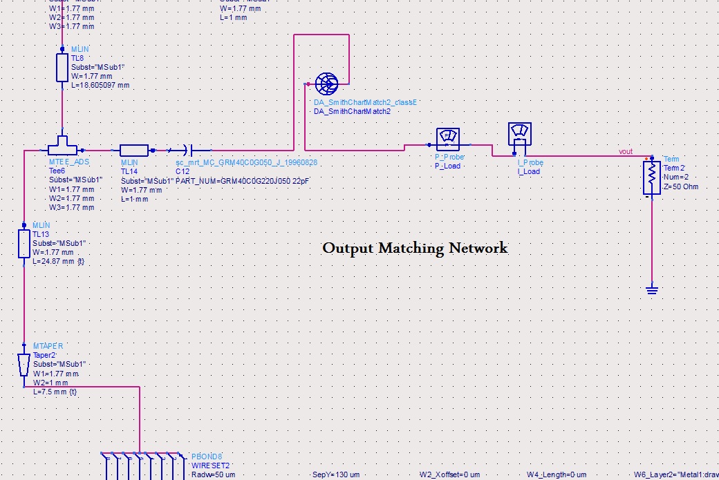
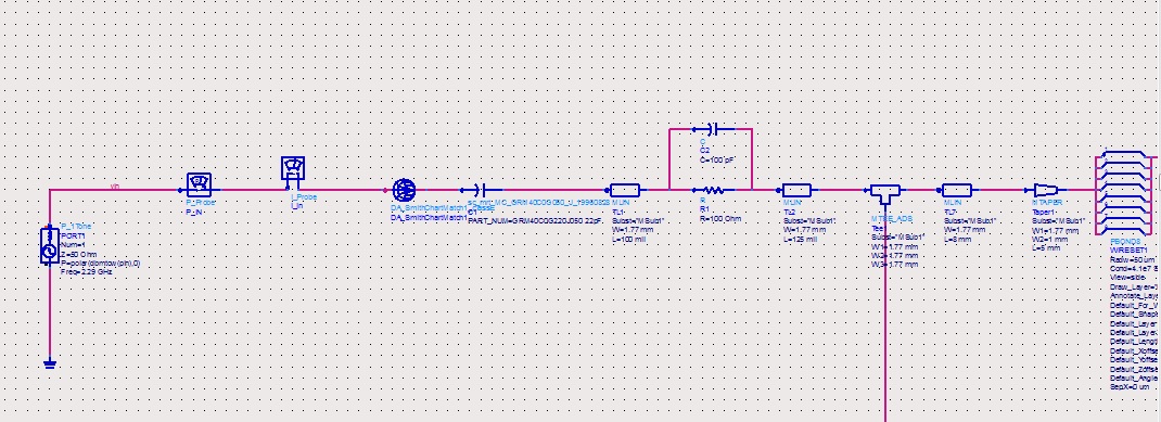
I designed the input and output matching networks with the above characteristics (below figures).
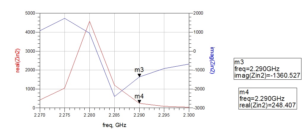
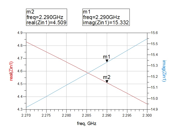
As you see at 2.95 GHz the matching networks work well. After I did simulation to see PAE and Pload, the results are so different to Pload=44dBm and PAE=64% (PAE=1.5% and Pload=-50dBm). I took a look on input matching (near the source not transistor) and output matching (near the load not transistor) they are not 50 Ohm at all! It means if I connect zload=4.5-j15.32 to output matching network, I will have 50 Ohm at output of the matching network, but if I connect the output of the transistor to the matching network I will not have 50 Ohm. The same problem is for the input matching too. You can see their behaviour below:

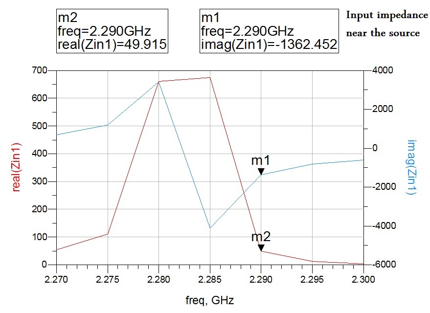
What is the problem? why cannot I get the PAE and Pload calculated by load pull analysis? Why are input and output matching networks not matched to 50 Ohm?
There are some fundamental errors in your simulations.
-Since the optimum output impedance is defined ( or is found to be ) , input impedance has less contribution into power delivered to the load and it's obvious that this impedance is not realistic that proves my treatment.( 250 Ohm+j*1360 Ohm=250 Ohm series within 74nH that is impossible input impedance for an active device)
-Optimum Load impedance is which must be seen by transistor itself but there are some other distributed components before matching circuit, ?
-It's same for input side...( But they may be ignored for the time being )
Thank you BigBoss.
"Since the optimum output impedance is defined ( or is found to be ) , input impedance has less contribution into power delivered to the load and it's obvious that this impedance is not realistic that proves my treatment.( 250 Ohm+j*1360 Ohm=250 Ohm series within 74nH that is impossible input impedance for an active device)" Okay, but what should I do?
"Optimum Load impedance is which must be seen by transistor itself but there are some other distributed components before matching circuit, ?" As it is obvious in the figure below, I have affected bondwire behaviour and a taper which changes 1.77mm width to 1mm width and a line which connects the taper to load and dc drain bias (they are needed). The impedance seen from the transistor to end of the TL13 is 0 nearly (I have adjusted it).
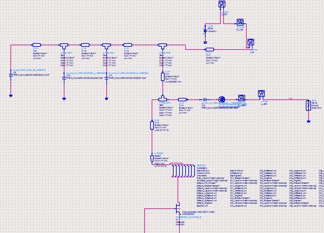
Small signal Input Impedance of the transistor should be matched to simply 50 Ohm( for the time being) .Don't consider input side and don't move them during load optimization.
All components which are connected to to Drain of the transistor must be included into this optimized impedance.So that when transistor looks through the his load, it will exactly see the optimum load impedance.Even a small element/impedance or something else would change this and it wouldn't work..
I hope you have found this optimum impedance without any matching or non-ideal bias circuit, it just has to be single transistor..
BigBoss,
Small signal Input Impedance of the transistor should be matched to simply 50 Ohm( for the time being) .Don't consider input side and don't move them during load optimization. (Okay, I have done it)
All components which are connected to to Drain of the transistor must be included into this optimized impedance.So that when transistor looks through the his load, it will exactly see the optimum load impedance.Even a small element/impedance or something else would change this and it wouldn't work.. (I have considered them in my simulation)
I hope you have found this optimum impedance without any matching or non-ideal bias circuit, it just has to be single transistor..
I did not have use matching, but I have used two bias circuits for Drain and Gate bias.
If I upload my circuit here, could you please take a look on it?
OK post your archived project file with nonlinear model here..
I have attached my simulation, nonlinear model and Ic characteristics. As I said before, I matched the input to 50 Ohm, then I used load pull analysis to find load value. Then I simulated my circuit but, I never see the PAE and Pload calculated in load pull analysis. Besides, the input is not matched anymore and output does not have matching too even after load pull analysis. It seems load pull analysis neglects output matching and just try to show a network which can satisfy the power and PAE we want.
You are still using output matching circuit....
You have to check the optimum impedance without output matching circuit.There will be just the transistor and its biasing circuits.Input may already be matched with a proper circuit technique, no matter...
But the output should be examined without ANYmatching circuit otherwise whet does the Load Pull make sense ?
You will find the optimum impedance then you will design a proper matching circuit in according with this impedance, that's it...
Output biasing circuit should not impact this impedance as well as possible and this impact must be minimum
I repeat here again, don't use any output matching circuit, just the transistor and non-impacting bias circuit.Evenmore, a ideal bias circuit...
Otherwise it doesn't make sense to search optimum impedance..
Thank you BigBoss. I did not use output matching circuit before load pull analysis. First, I designed bias circuits for drain and gate. Then I designed an input matching circuit. Then I used load pull analysis and found the proper impedance for load. After that I designed an output matching circuit and what you see in my simulation is output matching after load pull analysis not before it.
The point is load pull shows the proper impedance for high PAE and Power, but it neglects the output matching to 50 Ohm. I mean after doing load pull we will have a high PAE circuit, but its matching to 50 Ohm is terrible! (as you see in my simulation)
When I run your zip file in ADS2012 with bondwireutility_dkit_0.9 lib, and met the error:
"Error detected by hpeesofsim during netlist flattening.
Unresolved references:
Shape2_Rw
Shape1_Rw"
Who can help me on that?
For f_t issue, 1st I guess he optimize the bias circuit length, so a little change in the main circuit, the bias changed. f_t should find the basic bias theory from textbook.
