RF LNA design help is needed (ADS)
Im designing a LNA using ADS.
I have designed my single stub matching network and I use short circuit stubs in my design. I am getting a negative gain and I m confused about this.
If anyone can help on this it will be a great help.
What do you mean by "negative gain"? do you mean it's negative in dB, or the linear gain is negative?
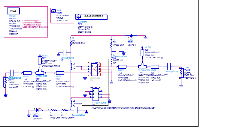
yes . its negative in dB I can attach the circuit here
yes . its negative in dB I can attach the circuit here
What about the gain without matching elements? Is it above 0dB?
yes it is.
Please check your connection, do you get them right?
You made shot connected the drain and the gate by stubs...
Place DC blocking capacitors before matching circuits because short stubs make the gate and drain short circuit..
Also, the length of the shorted stubs makes no sense to me. They are very short (~2mm) and I don't think this is the correct length for impedance matching your transistors.
In this linear simulation, the bias supply doesn't have an effect, but that looks wrong. As Bigboss mentioned it is shorted to ground, and the entire configuration makes no sense (two 5V sources, R3 in series with R4, wrong gate bias voltage).