How to do the em-cosimulation of a CPWG circuit board?
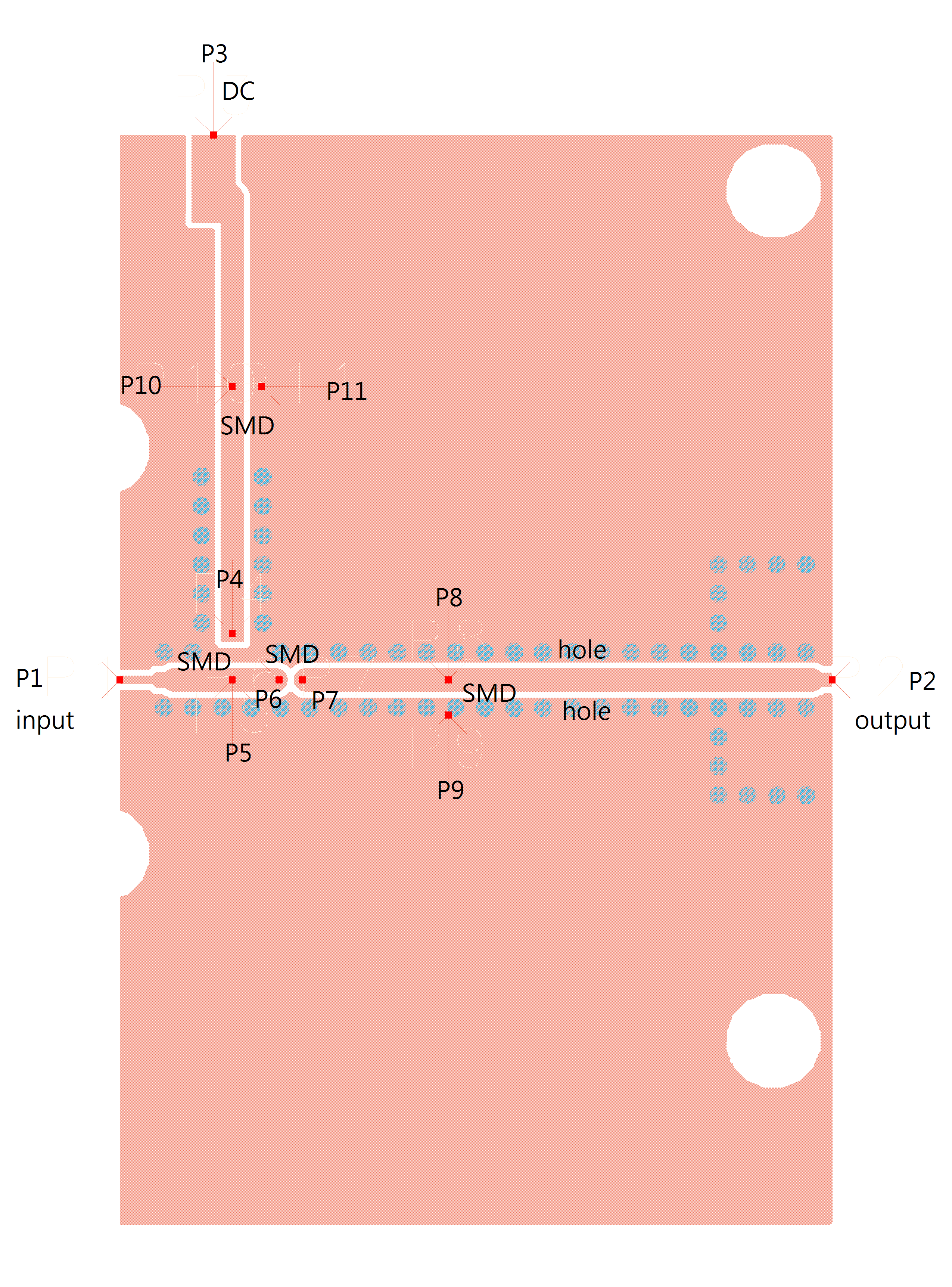
Please see the attached picture(layout.png), and that's the output matching of the power amplifier circuit.

I have set 7 port.
Port1(P1),Port2(P2),Port3(P3) for input, output,DC bias
Port4(P4+,P5-),Port5(P6+,P7-),Port6(P8+,P9-),Port7(P10+,P11-) for placing SMD components.
My substrate is as (substrate.png),

For the CPWG substrate, I have few questions:
1. For the cond, I don't know what is the difference between "sheet" and "Intrude into substrate" ?
2. Is it right to place via at substrate to let the metal beside the signal metal be grounded?
For the port calibration,
I've set "TML" for the input,output,and dc port, and set "SMD" for the ports which are for placing the SMD component.
I set the em simulation frequency from 0~2GHz, but when the simulation start, there are some warnings:
"Layout healing changed the layout. The actual
highest aggregate snap distance was 0.04 mm.
Further details have been written to the DRC
report."
"The port setup needed to be corrected:
Calibration will not be used for port "P6" (pins
"P4" and "P5" are not on the edge between a
conductive and a nonconductive region)."
And all the SMD ports have the same message.
I change the calibration "SMD" to "None", and there is only the first warning left.
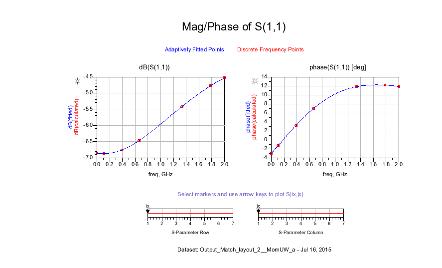
The result is as (result.png)

I don't know why can't I choose SMD calibration?
Besides,the result only shows S11,but I have more than one port!?
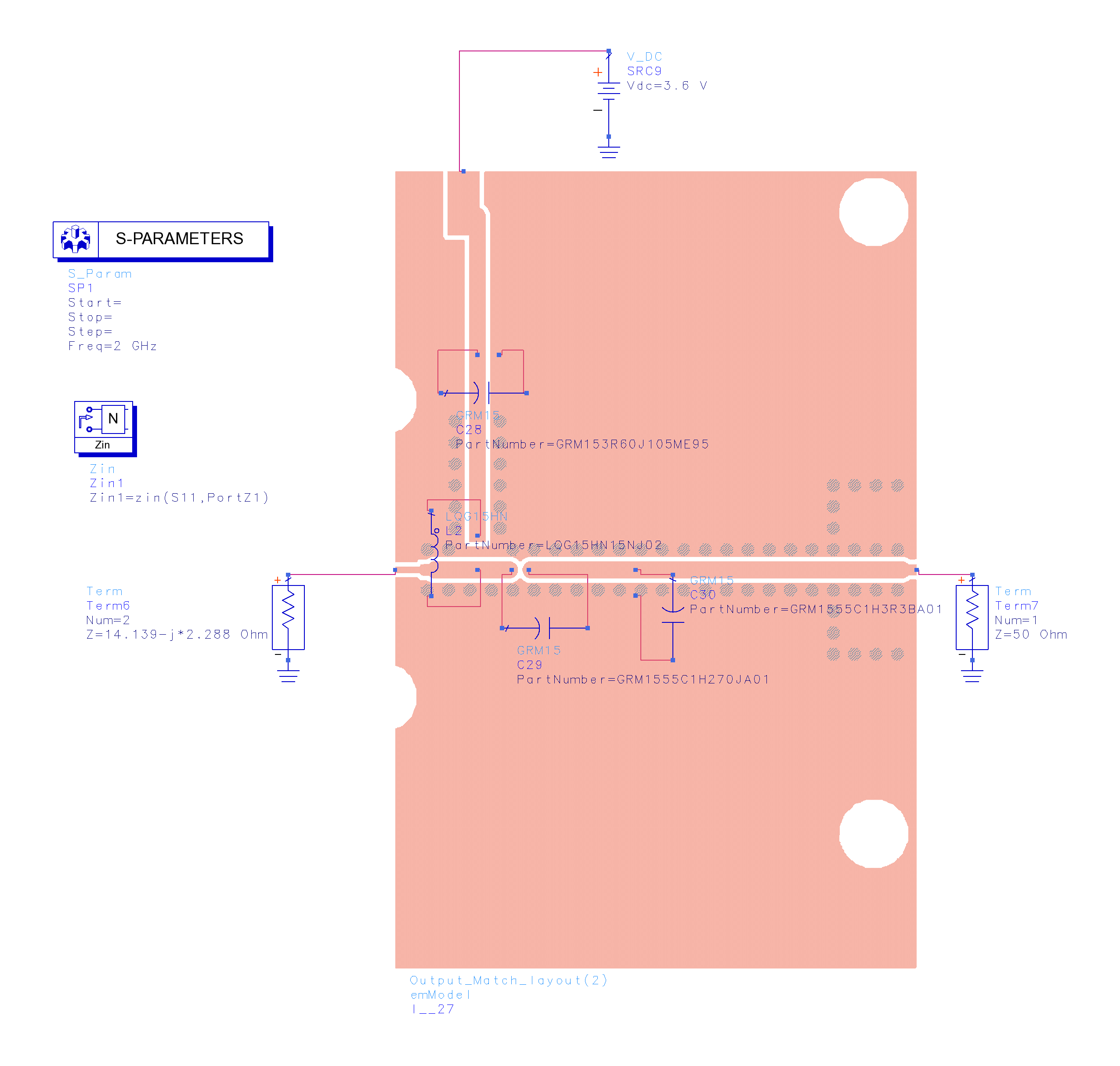
My final goal is to simulate the schematic and see the Zin at 2GHz.(final.png)

But it has an error:
"Error detected by hpeesofsim during netlist parsing.
`(' illegal: valid characters in design names are alphanumeric or _`@#&+-=^
define "Output_Match_layout(2)" ( P1 P2 P3 P4 P5 P6 P7 P8 P9 P10 P11 Ref=0 ))
But I didn't change the Pin name.
Does anyone have idea?
Thanks for replying~~
ps. I've attached my workspace.Outputmatching_wrk.7z
You must choose many suitable gnd vias spaced by L/20, and suitable dielectric such as polyamide or Teflon and thickness of dielectric ~1/2 of line pitch (track & gap).
More details.... https://www.hittite.com/content/docu...components.pdf
Thank you,SunnySkyguy, and I'll check the document.
I've figured out the error message:
"Error detected by hpeesofsim during netlist parsing.
`(' illegal: valid characters in design names are alphanumeric or _`@#&+-=^
define "Output_Match_layout(2)" ( P1 P2 P3 P4 P5 P6 P7 P8 P9 P10 P11 Ref=0 ))"
It's because of my cell name "Output_Match_layout(2)" which have "()".
When I change it to "Output_Match_layout_2", it can simulate properly.
But I am not sure whether the result is correct or not...
Back to the layout,
for the CPWG substrate, I still don't know the difference between "sheet" and "intrude to the substrate" fot the top metal.
for the em setup, I don't know why it shows the warning:
"The port setup needed to be corrected:
Calibration will not be used for port "P6" (pins
"P4" and "P5" are not on the edge between a
conductive and a nonconductive region)." when I choose SMD calibration.
I think maybe I should try the edge/area pin other than single pin.
By the way, it's my misunderstanding. The result has a slide below to change the S parameter.
