Problems with ADS EM-cosimulation and schematic results for CPWG structures
时间:04-04
整理:3721RD
点击:
Hi ,
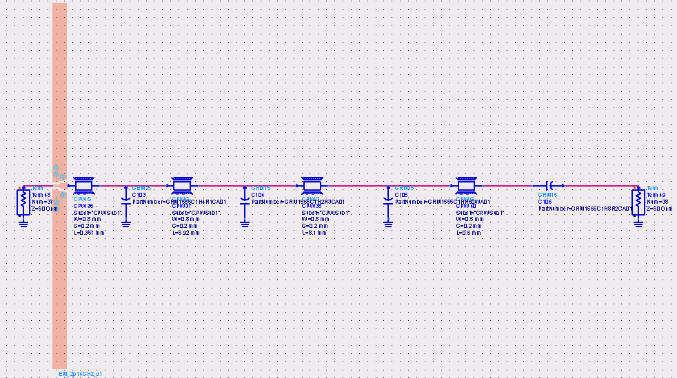
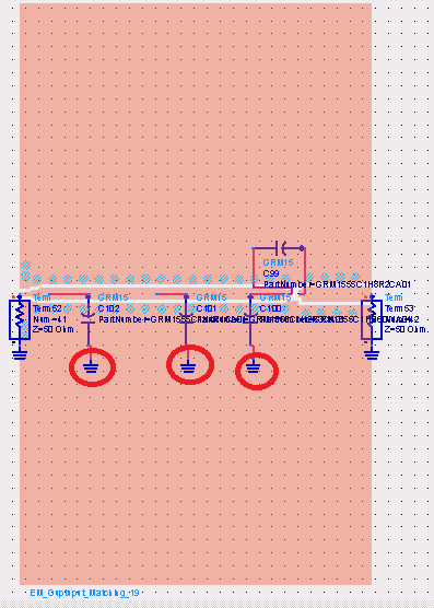
I have designed the output matching with CPWG(cpw with ground) line and L,C component.
But the result of EM-cosimulation looks strange and different from the result of schematic.
(S(37,37) is for schematic, S(39,39) is for EM cosimulation)
I found the problem.
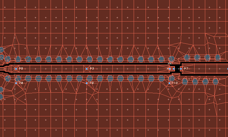
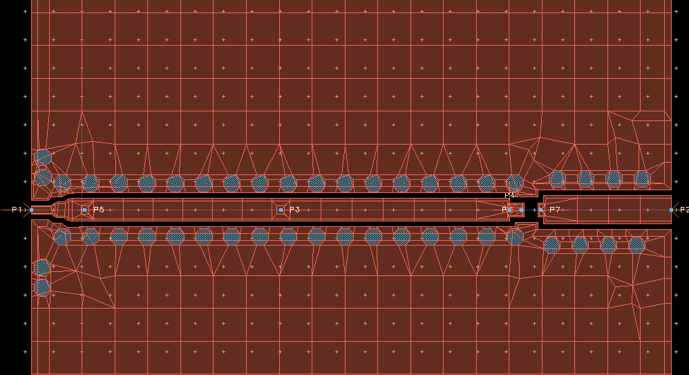
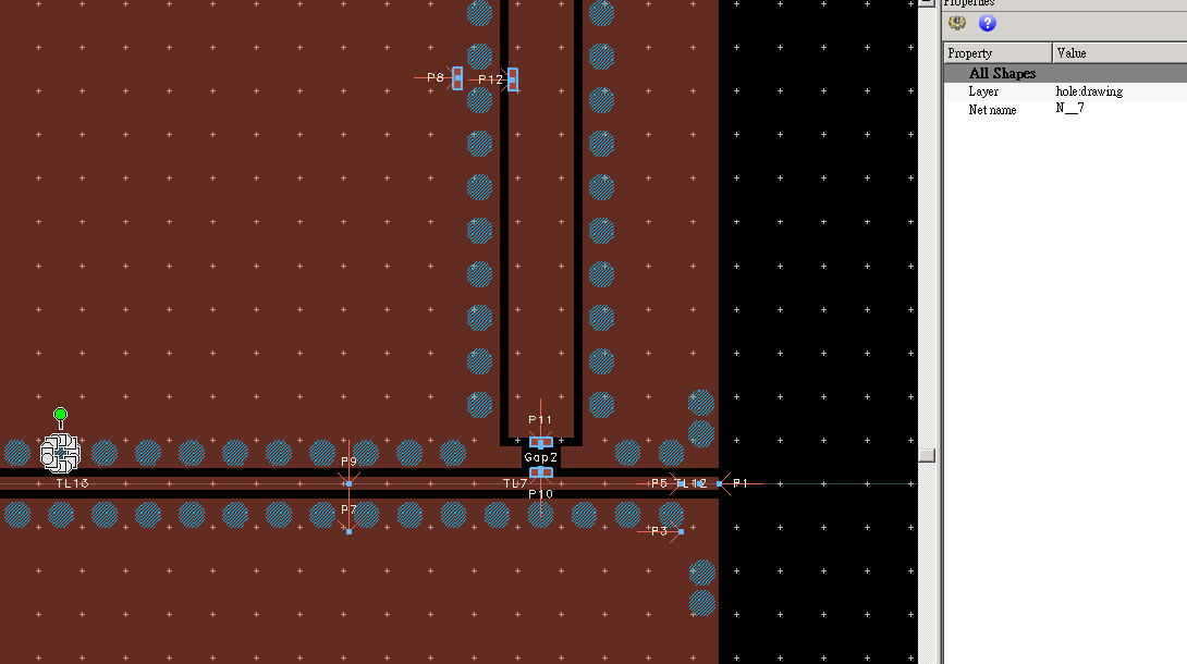
When I took away the pins on the ground of the CPWG line on my layout, and let the capacitor connected to the ideal ground, the result seems less strange, but is different from the original result.
(S(37,37) is for schematic,S(39,39) is for EM-cosim with ground pin on layout,S(41,41) is for EM-cosim without ground pin on layout.)
Does someone know if I should add the ground pin on the layout?
I have designed the output matching with CPWG(cpw with ground) line and L,C component.


But the result of EM-cosimulation looks strange and different from the result of schematic.
(S(37,37) is for schematic, S(39,39) is for EM cosimulation)

I found the problem.
When I took away the pins on the ground of the CPWG line on my layout, and let the capacitor connected to the ideal ground, the result seems less strange, but is different from the original result.


(S(37,37) is for schematic,S(39,39) is for EM-cosim with ground pin on layout,S(41,41) is for EM-cosim without ground pin on layout.)
Does someone know if I should add the ground pin on the layout?
Change the values of capacitors a bit and see if it matches,your schematic results.
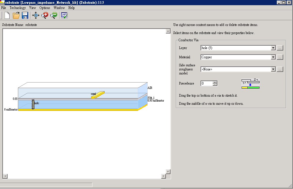
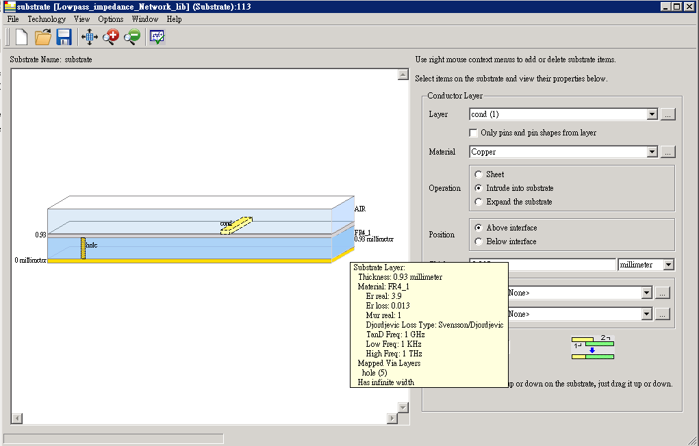
If the frequency is too high, check the VIA specifications in substrate file. EM simulator does probably not take the VIAs properly into account.
What do you mean that EM simulator does probably not take the VIAs properly into account?
Is my substrate setting right?

EM cosimulation Problems 相关文章:
- I/Q baseband Modulator Demodulator
- ADS schematic to layout
- NFC System with antenna which can provide from 1 A/m to 7.5 A/m signal strength
- Why are all reference sensitivity requirement of all bands different in WCDMA (UMTS)
- itemdef.ael not found while trying to place a SmithChart smart component
- Using ADS2019, How to set and measure tempature values for LNA?