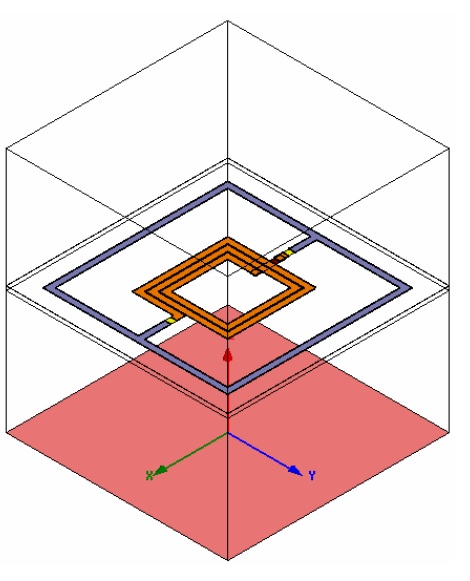
Gnd connection for chip inductor

No. Ground is whatever you use/connect for ground return, and this is always on the top side of the chip. The bottom side is floating.
Thanks! Should this be a ring/closed loop itself? How do you choose the width of the gnd conductor or distance of gnd ring from the inductor?
The ring represents a closed metal boundary in the chip, where return current can flow in real hardware. So that gives you the dimensions: same as hardware. It is important to understand that this ring forms a shorted secondary loop around the inductors, so it has some negative effect. Unfortunately in HFSS you can't model inductors without such a return path, and on chip (hardware) you also need some return path.
The trick is to have "enough" distance between the inductor and the ground frame, and "enough" depends on multiple factors like number of turns etc. Note that larger distance from inductor to ground ring also means longer feed lines, which are included in results and degrade the Q factor.
Sometimes designers use a slotted frame (not closed loop) when inductors have both terminals on one side.
This inductor designs is somewhat tricky, and it can take time to get a feeling for "good" methodology.
Can I take Rdc = re(1/Yin) at 0hz in this design?
If you want to measure the resistance of the full path (including return path in ground frame), then yes.
Obviously the width of your ground frame matters in this case.
connection Gnd inductor 相关文章:
- How to achieve wireless connection between a resonator sensor and VNA?
- Keysight ADS ground connection in schematic not reflected in layout
- Do you know the basic specification requirements for optical fiber connection?
- SMA bad connection mismatch in PCB from 6.5 GHz (measurement and HFSS simulation)
- S2P file with Balun Connection
- Modify wireless keyboard to use wired connection
