PCB Layout consideration for Walsin antenna
时间:04-04
整理:3721RD
点击:
Hi,
I have a custom board with bluetooth. I have used RFANT321620A1T antenna from Walsin.
Data transmission and reception is happening properly but the range of the antenna is less.
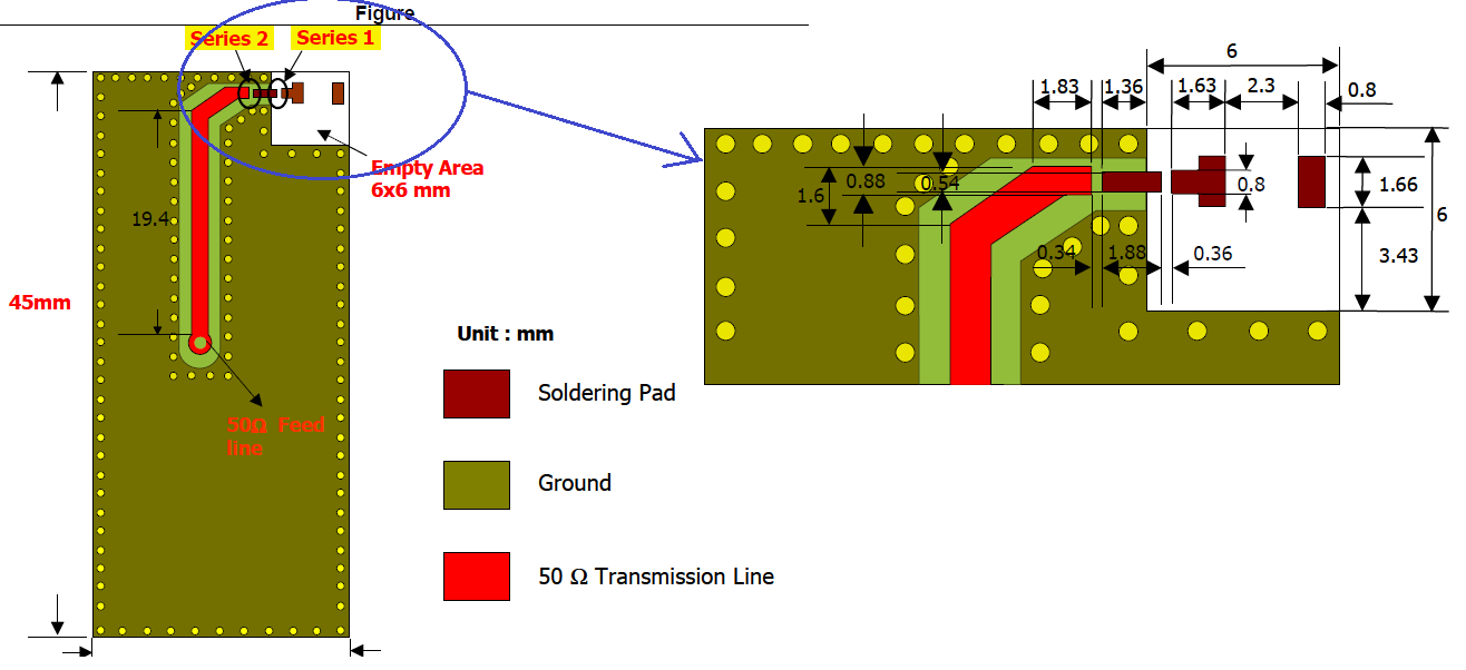
While going through the datasheet, i found the following figure which provides the PCB guidelines.
In the place where it says Series 1 and Series 2, there is a gap in the connections, is it supposed to be like that? or Am i interpreting it wrong?
Thanks
Arun
I have a custom board with bluetooth. I have used RFANT321620A1T antenna from Walsin.
Data transmission and reception is happening properly but the range of the antenna is less.
While going through the datasheet, i found the following figure which provides the PCB guidelines.

In the place where it says Series 1 and Series 2, there is a gap in the connections, is it supposed to be like that? or Am i interpreting it wrong?
Thanks
Arun
Typically, these are for SMD elements for matching. If no matching network is needed, you can use 0 Ohm resistor to make the connection.
Layout PCB consideration 相关文章:
