RF PIN diode switch explaination
Could someone please explain,
What is the difference between a PIN diode switch and a tuned PIN diode switch?
I did some googling, cant find any specific reference text to a tuned pin diode switch
do you have a reference ?
I found it on here:
http://www.ieee.li/pdf/essay/pin_diode_handbook.pdf
Page 8 it talks about tuned switch but what do they mean by tuned?
Tuned means involving a resonant circuit or a transmission line stub matching the operation frequency.
yeah, was thinking that and that is the case for the majority of times pin diodes are used for TX/RX switching to an antenna
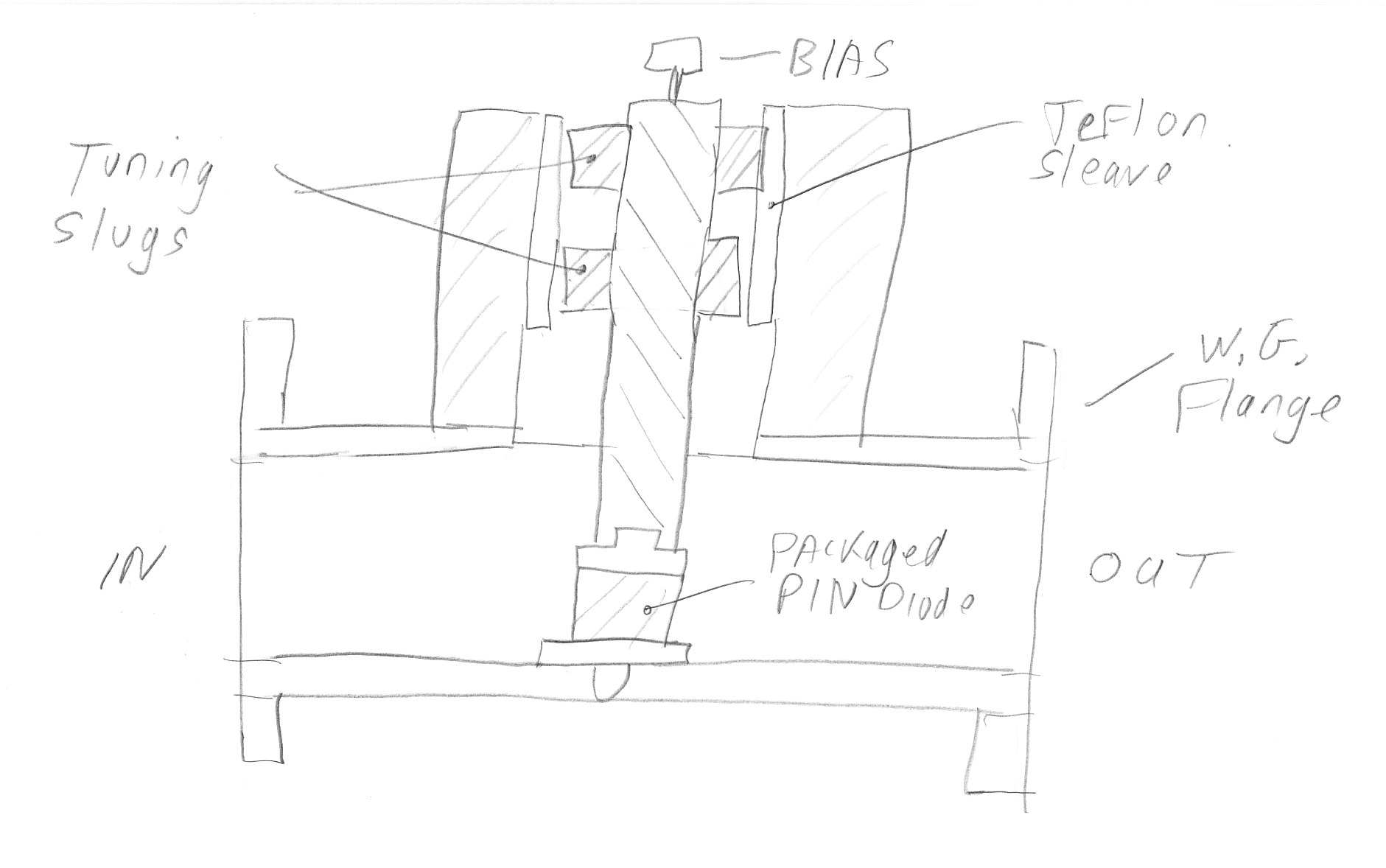
Back in the day....when all microwaves used WAVEGUIDES and diodes were in tall ceramic packages with pretty large package inductances....it was hard to get those packaged diodes to reflect signals when they were forward biased. Then some bright guy thought "Hey, could I use a coaxial bias network to add an effective series capacitance, reactive cancelling-out the package inductance, and get a near perfect short circuit across my waveguide? That would give me at least 35 db isolation per diode!". and that is what he did, he "tuned out" the package parasitics.
But, like anything matching out a reactive part, it had limited bandwidth. That is why today we use pin diodes with the absolute minimum package reactances, and no longer try to "tune them up".
You might still run into this in a high power waveguide switch...especially if it uses stacked pin diodes to handle high power.
Uhh.. so "tuned" pin diodes are used as a impedance matching circuit? or its a switch with no reactance (imaginary part of impedance)?
Not impedance matching...you want the shunt pin diode to look as much as an open circuit as possible when it is reverse biased.
But you use the bias structure to "tune out" the package parasitic inductance, so you get less signal leaking past the forward biased pin diode.

The slugs are moved up and down the bias pin until maximum isolation is achieved with the diode forward biased.
