Power Amplifier Design for Bluetooth Applications
You need to design a mixer which upconverts the baseband signal using the VCO output. The output of the mixer should go to the PA. Start with class AB topology and based on the output resistor you are driving, do the calculations to find all the parameters like output swing and LC tank values etc.
I was told by my professor to connect the vco to the PA because that is how the bluetooth architecture is supposed to be.
OK then are you modulating the vco output? And what kind of modulation are you designing the circuit for?
All I have done right now is a vco design. I dont know where to go from there
Either you need a mixer for upconversion or you need to generate a modulated VCO output(in case you are directly connecting the VCO output to PA) in order to be able to transmit using PA.
oh i guess i neeed to look more into it
One simple option for a Bluetooth amplifier is to use a cheap BFP450 transistor.
http://digilander.libero.it/giovanni...ss1/class1.htm
http://www.infineon.com/dgdl/Infineo...14275d537d074b
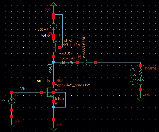
So I am just trying to build the power amplifier on its own for now using the class A topology. I am not sure how to run output power and output p1db simulations on Cadence ADE. I was able to run output p1db but I am not sure if my setup is correct. I had just one port, which was placed at the output and then I ran a PSS simulation and plotted the output 1db compression of the port. Can anyone confirm that that is how to run the simulation? Also, what are ways to get better output p1db, as i need to have above 3dbm.