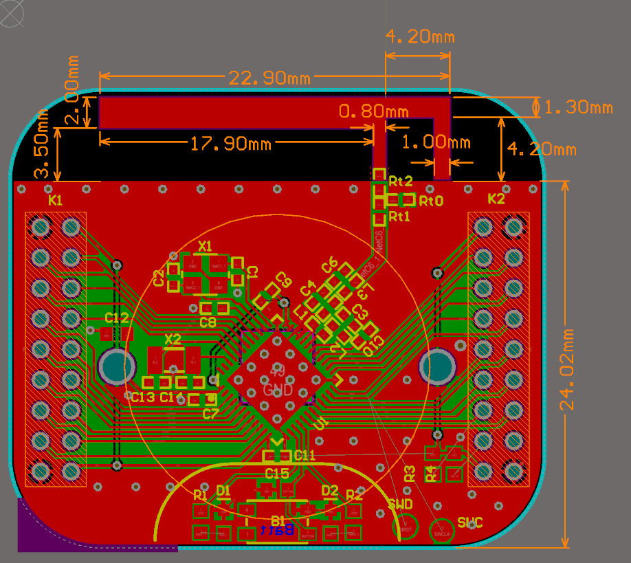
Bluetooth PCB inverted F antenna design
Here is the design layout (the tail connects to ground, just doesn't look like it here). I've still to do via stitching, but I want to finalise the antenna first.

I know antenna design is not a trivial task, but will this antenna work to my standards? if not, what might need modifying to make it perform?
Are there any alternative antennas out there that may fit my performance and spatial requirements? A chip antenna may be a possibility, but it seems many of them need mounted vertically and I don't have the space for that. I looked at a TI PCB IFA design but it's just slightly too large for the ~34mm x 5.5mm I have available.
Inverted-F antenna it will work better than most of chip antennas.
Your inverted-F design should work fine, mainly because you have available a solid ground under the antenna (which is a main requirement for this type of antenna).
The antenna might need some input impedance tuning (S11), but I see that you already have in place 3 components for this task. For S11 tuning, ideally would be to have access to a Network Analyzer.
I hoped this would be the case. The main problem is I suppose, I have no idea just how well it will work. I don't know what the bandwidth will look like or what sort of output power or directionality it might have. Complicated business it seems!
The bandwidth of inverted-F antenna made on standard FR4 should be just fine for a Bluetooth requirements.
In fact, this antenna is one of the simplest PCB antenna type, having decent performances.
As I said, a Network Analyzer would give you information in terms of input impedance and input bandwidth (S11).
Also if use the NA in a radiated setup (reference dipole antenna replacement) gives you information about antenna gain and efficiency vs frequency (S21).
You do know that trying to design an omnidirectional PCB antenna is a fool's errand, don't you?
If you can not measure radiating characteristics concentrate in matching. Get it matched so S11 < 10 dB across your all band. This gives you reasonable assurance that all transmitted energy went into the air. Pattern may not be exactly omnidirectional but close enough.
If you like challenges match antenna without lumped components - adjust position and width of the stub, position of feed point. This result in some further improvement of efficiency.
