what are some ways to implement very high impedance transmission line
I was trying to design a 2GHz microstrip filter. It's has 4th order butterworth response. For this filter I require a stub that has 0.036 mm thickness. This is very impractical for the PCB house (I am going for a cheap PCB manufacturer). Is there any other structure that can maintain very high characteristic impedance while being practical. For example, as far as I know radial stubs are used for very low characteristic impedances while being relatively small compared to regular stubs. Is there any shape or trick for high impedance transmission line?
Approximately 0.13mm is the minimum trace width for cheap PCB houses. With that width, use a thicker substrate (up to 2mm thick). About the highest Z line you can get is 160Ω.
Try a different filter topology.
The only option to get highest impedance line is to make it thinner as possible, because the height of the substrate is pretty much limited.
I think the thinnest trace made by cheap PCB houses is 4 mils (~0.1mm). At least the manufacturer that I use for personal circuits does this.
Not big difference from 0.13mm, but good to know.
Thanks for your responses. I guess I have not other way, but to try different topology because I require 217 Ohm characteristic impedance,which is very unpractical for the PCB house.
you could try a wire, or wirebond. Since it is above the substrate with partial air dielectric, it will be higher impedance. or a better way to think of it, it would look more like a lumped element inductor.
also possibly a coupled line structure:

from page 215 matthaei young and jones
There's more than one way to skin a cat. What response do you want - LP, HP, BP, BS? Is the 2GHz figure the -3dB cutoff, center freq, or what?
Do you have the option of removing the ground directly under the high Z line. Coplanar Waveguide possibly?
you could even punch out a square hole in the substrate, and solder a thin wire over the open air gap
It's a 2GHz (-3dB) lowpass filter. I designed it using richard's transformation kuroda's identity.
That's an interesting suggestion. Can you elaborate more or suggest me a document to read? The filter is a microstrip filter. Is it possible to design a filter which incorporates both microstrip and coplanar waveguide structures? Last question, is it easier to design a high impedance line with CPW?
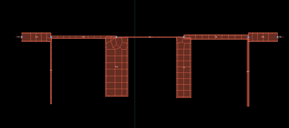
Here is the picture of the filter. The right most open stub is the one that is causing the problem (it's 0.036mm wide). After running optimization and tweaking the length of this stub and 3 the lengths of transmission lines that are connecting the stubs I managed to get very good response with practical width (0.5mm). But what if I want 200 Ohm characteristic impedance transmission line, I still want to know how to do it.
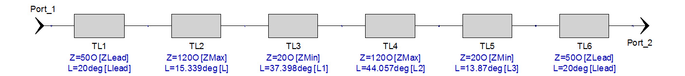
Here is a design using a stepped topology (NOTE: the Ω symbol came out as an O):
Here"s the response:

Richard's transformation utilizes 1/8 wavelength lines at the corner frequency. If you choose a 1/16th wavelength line for the high Z line, you can use a wider line and re-optimize! This should work if you are not relying on the 1/8th line to provide a zero far out of band.
Dirty solution is: Set the width/length range of the traces you can accept, and set the in-band and out-band performance targets, then optimize all the parameters, almost you can get what you want.
Here's another take on your problem. I used a 7th order Butterworth filter for symetry.
Design:

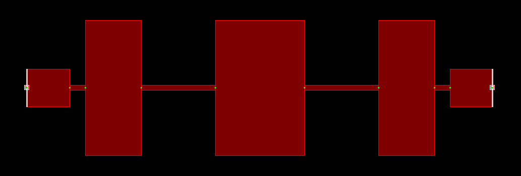
Layout:
Response:

Thats what I exactly did.:D It works but I am not satisfied.
Even if the TL could be fabricated somehow I bet it would radiate so much that it wouldn't work nearly as much as expected.