results do not match with datasheet
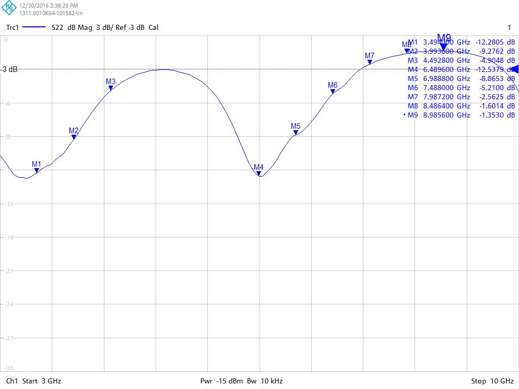
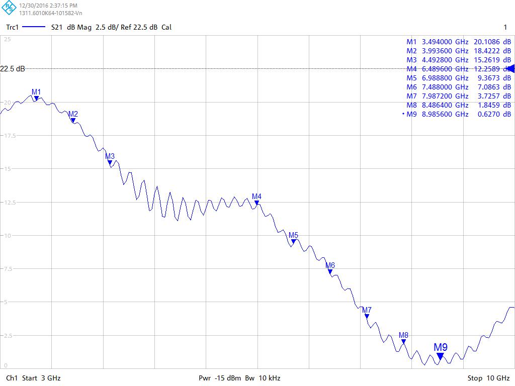
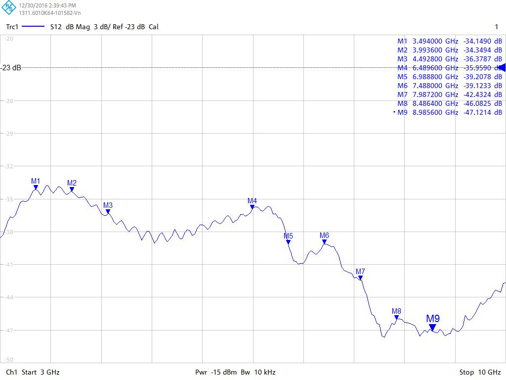
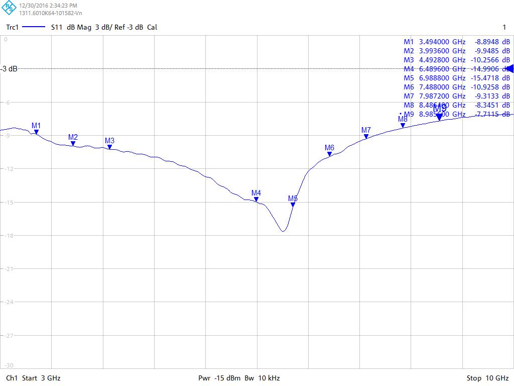
Most obvious point is S21 dropping to about zero gain at 10 GHz compared to 18 dB with the reference design. Suggests unsuitable layout and/or bias T. Show your design.
can i not try with simply playing with the matching components that have been used in the developement board design, i am using the same matching components.
In my understanding, the development board doesn't have "matching components" just a bias network designed to have little effect in the 3 to 10 GHz range.
I don't know if the layout or the components make 10 GHz gain drop to zero in your design.
S22 looks much worse than S11 on top of the S21 mentioned by FvM. I would be very suspicious of something on the output (assuming your line is good 50ohms for 10GHz).
I think your LNA is oscillating
i had used a poor cable(connected to board sma from lna ) in my previous measurement, so just to make sure that nothing is wrong with the measurement going to check with rf cables.
i checked my results again this time using a better cable to sma, now both the port response do not match with the datasheet response.since i used the same board i was not expecting the port 1 performance to get effected. since there is no change at port 1 side.
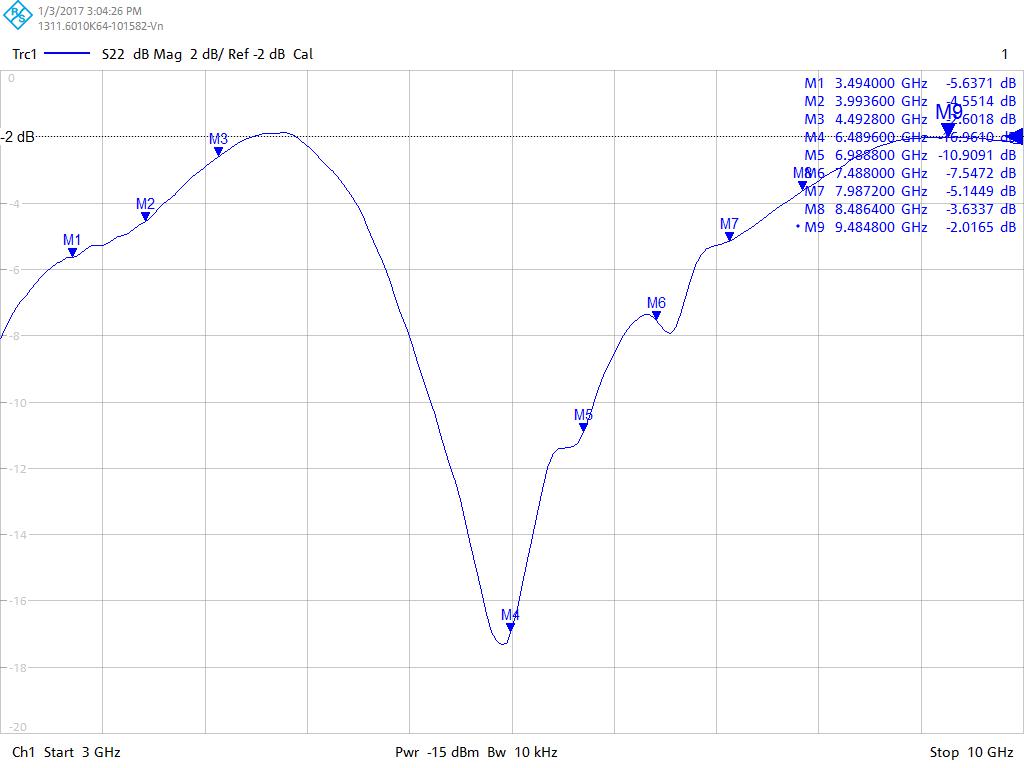
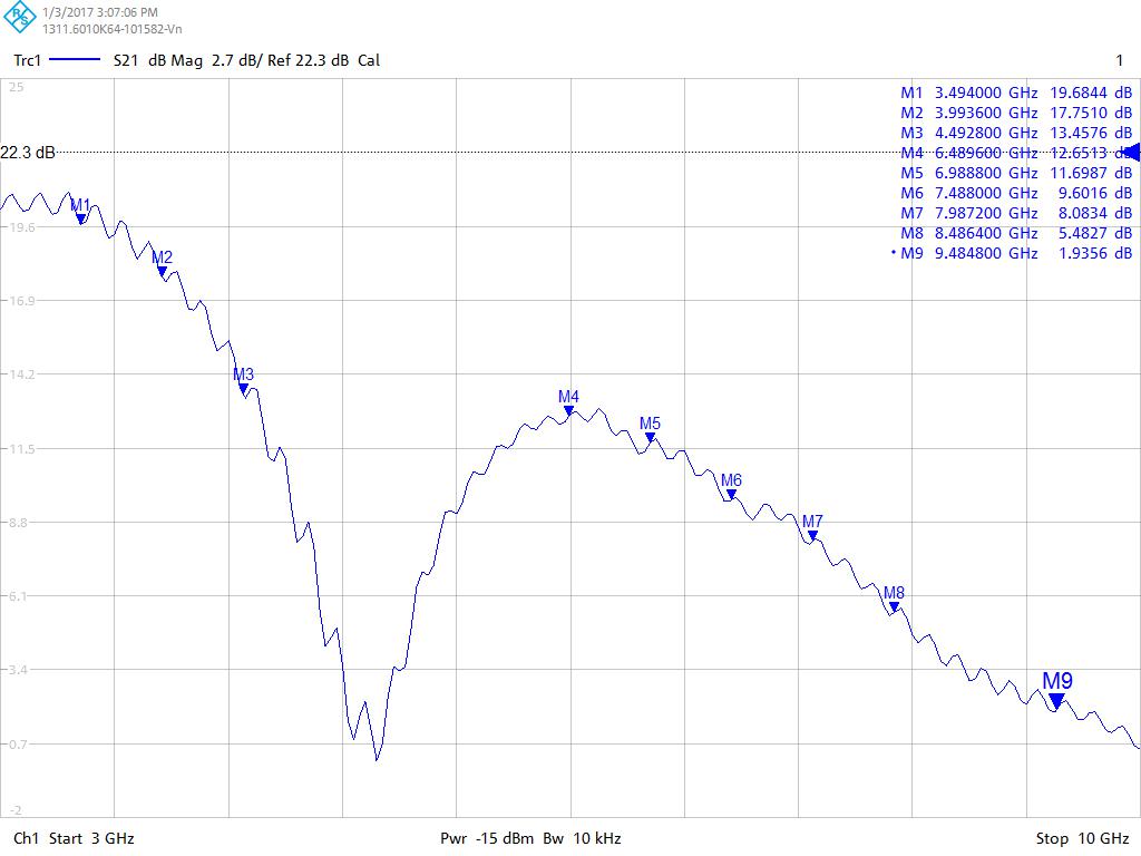
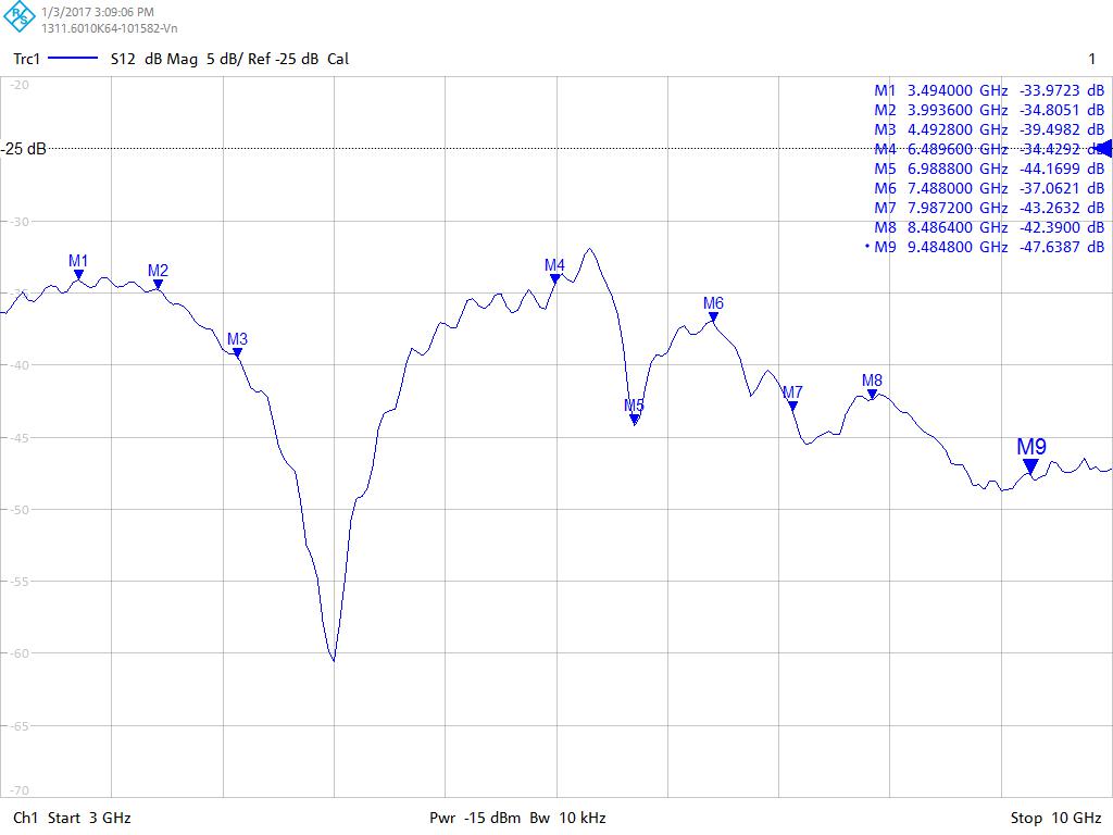
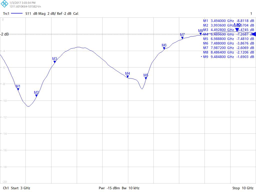
The new results are in some regard even worse, showing now a S21 drop to nearly zero dB around 5 GHz.
My post #2 question is still pending.
The "poor cable" point makes me also wonder if the VNA setup has been regularly calibrated.
we have a uwb chip which is connected to this lna (along with the referred matching as given in the datasheet ) and then it is given directly to the antenna. no other components.
so on your post 2 regarding the "drop in the gain" since no other components were used in this path, we were not expecting the performance to be this much bad in the recommended frequency range.
also since we have started testing the board now i do not have sufficient data, so i thought s parameter can give pretty good idea. now i am thinking to measure the received power after this lna just to make sure that the problem is in lna block (matching or layout, if it exist even after changing the components than can be more sure that it is happening because of the layout thing as you said). although this same as s para measuement
also pretty sure that the network analyzer was calibrated because repeated the experiment twice from start just to make sure and got the same results also tried also lifting the board and the cable of sna whether any loose connection but the response was still the same, so yeah pretty sure about the measurement.
one thing which i am still puzzled about is that why the s11 got changed as nothing was done on it used the same board just with different cable.(already checked for any short).
can you recommend any measurement or test to confirm the layout or matching issue to be sure why the performance is so poor.
The "UWB chip" (I presume the Johanson 3-10 GHz device mentioned in a previous thread) must be disconnected in LNA S-parameter measurements. In so far I don't understand the relation of this comment. As previously mentioned, there's no actual "matching network" in the LNA reference design, just a bias-T with hopefully small effect in the frequency range of interest.
yes it is disconnected sorry for making it confusing.
the matching network i am referring to is the one they use in their developement board. i am measuring the s parameters by keeping those elements(s parameters across those). also they should not impact that large bandwidth.
is there any other test which you can recommend
Both input and output return loss is very poor above 8GHz. I would not expect good but what bias voltage are you using? Looking at the data sheet, return loss goes to crap below 3V. Sure your line widths and connectors are correct?
measured both vpd and vdd, both are above 3.03v
- diffrent results in hfss feko and cst
- Simulation in ANSYS of a paper do not get the same results?
- Wierd S-Parameter results simulating C-Band PCB traces in CST Studio.
- Lumped and Distributed Circuits results error
- Different Results in Transient Simulation with S-parameters from file in ADS
- Help with results of a Wirelles Power Transfer Circuit.
