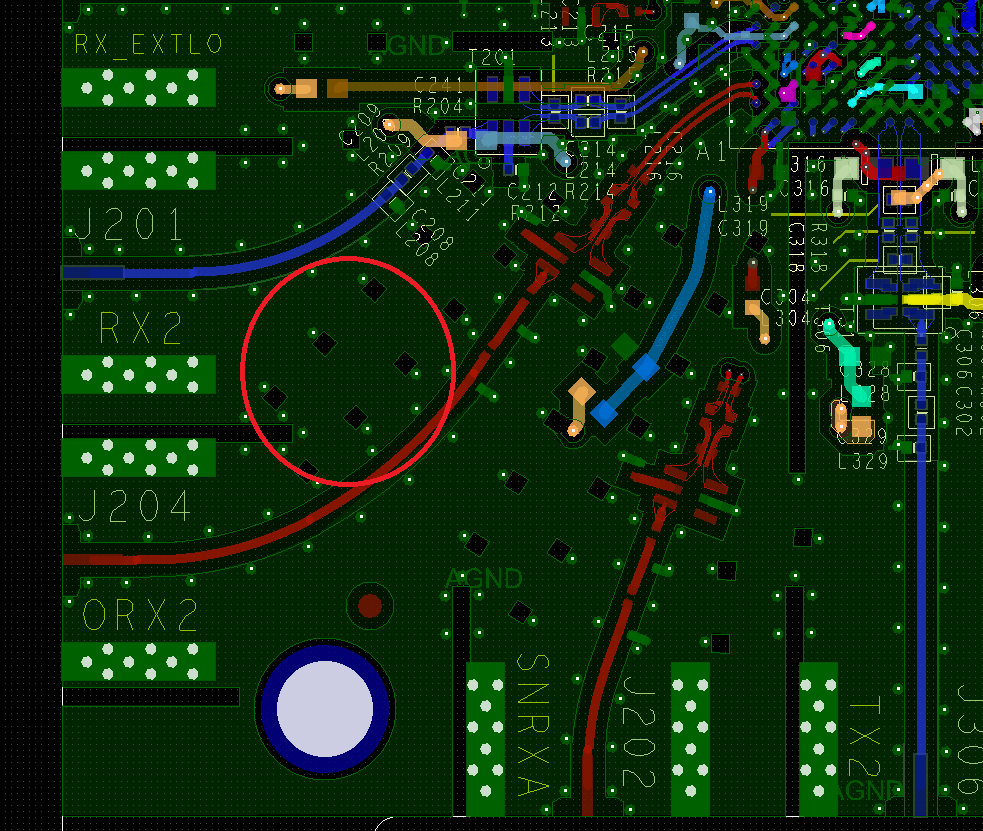
AD9371 EVB PCB design [vias each have a black square(copper removed) next to it]
时间:04-04
整理:3721RD
点击:
There are many GND Vias between RF traces, but In the middle of the GND plane, some vias each have a black square(copper removed) next to it.
What's the reason behind this design?
We are considering follow the EVB's design in our project.
Any help will be greatly appreciated!

What's the reason behind this design?
We are considering follow the EVB's design in our project.
Any help will be greatly appreciated!
The square apertures are said to work as isolation structure, advanced RF voodoo.... Everything verbosely discussed in the AD9371 "System Development User Guide UG-992", page 259ff.
By the way, it's a rather complex PCB stack-up, 14 layer Rogers/FR4 composite.
Thanks very much. I'ill read UG-992 carefully.
