S11 smith chart contour too big
Here is the both measurement and simulation results. What could be the problem here ?

It is not problem.
Simply you have no experience of actual measurement.
Can you understand followings ?
- Calibartion
- Reference Plane
- Port Extension
- Stimulus Power
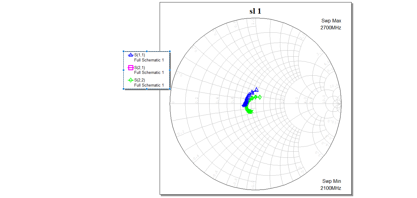
Frequency Range of your EDA Tool Play is following
Start=2100MHz
Stop=2700MHz
Frequency Range of VNA is following
Start=652.5MHz
Stop=2940MHz
Calibration of your VNA is not appropriate.
Do you surely activate calibration ?
Your locus seems to be non-calibrated data.
Where is a reference plane of VNA ?
Make Frequency Range of VNA narrower. e.g. same as your EDA Tool Play.
Then recalibrate.
Set same reference plane as EDA Tool Play.
Surely see VNA.
Set stimulus power of VNA lower.
yes, there are big electrical lengths at the input and output, and your device impedances are rotating all over the place as the frequency changes. You need to make a measurement, or a simulation, right at the terminals of the device to get the expected smith chart refleciton corefficiens.
You can tell that you have long FIFTY OHM transmission lines in the circuit as the circles are centered at the middle of the smith chart.