Cheap RF 433.92MHz design, PCB track antenna, values of capacitors
I'm doing a RF remote control project using a PCB with microcontroller and with simple onboard antenna layout as transmitter and a 433.92MHz receiver RWS-371F-6 model. Here is the datasheet of the receiver: https://www.es.co.th/Schemetic/PDF/RWS-371F-6.PDF
I don't have knowledge about RF design, just electronics and MCU programming. I'm using manchester encoding/decoding @ 1000bps to improve the communication distance from receptor board to the transmitter. 'RF-TX' is a 0V~5V signal.
The circuit of RF was copied from a board of a garage door opener, but I included my own microcontroller to the PCB schematic and I have some prototypes of the board. The values of resistors (150 Ohms, 47K, 47 Ohms) was also copied from the garage opener transmitter board. Here I am showing the layout of my board and the values/part number of the components. I've mounted a few pF capacitor combination values (0805) for C2/C3. I have a capacitor sample book with many values on pF range, many values from 1 to 22pF. The communication TX/RX is working correctly, but I want to check if I can increase the distance range by using adequate values for C2/C3. Currently I'm using both as 1pF.
At the receptor, I'm using coil loaded antenna with 1/4 of wavelength, the same of the picture, tomorrow I will try a straight rigid wire of 1/2 of wavelength.
Well, as said, my doubt is around the correct values of C2/C3, can somebody who understand of RF desing calculate them easily? Or does this generate a kind of service that I have to contract a RF designer to calculate them to me?
Regards.

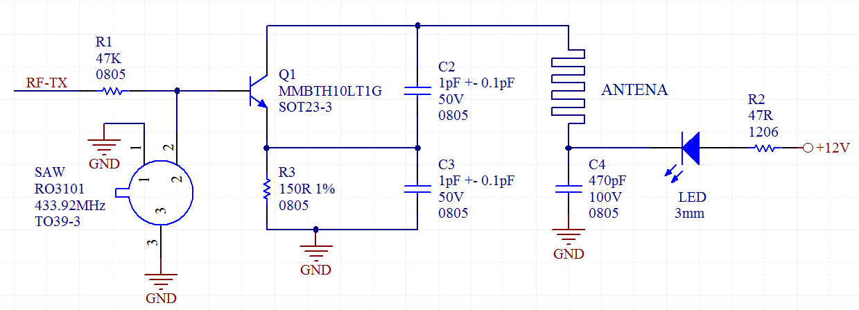
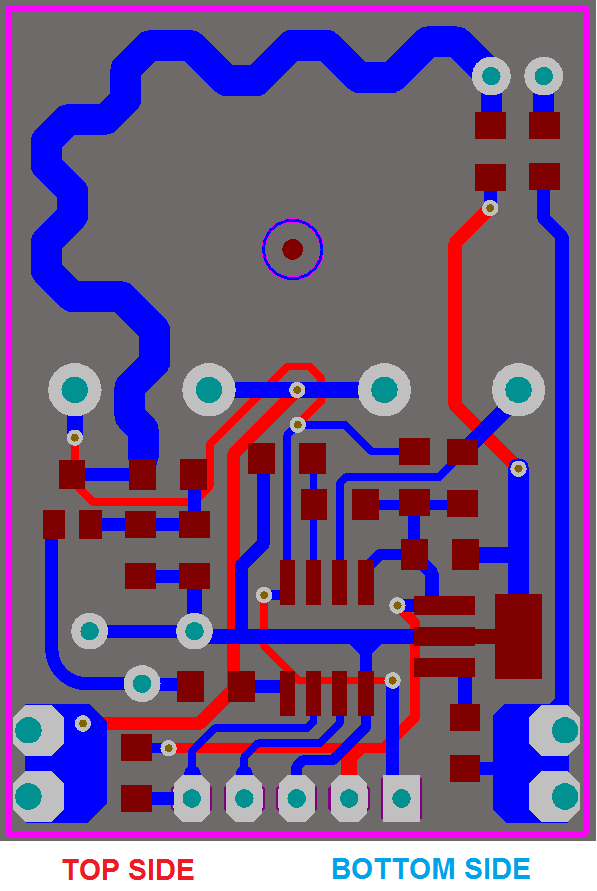
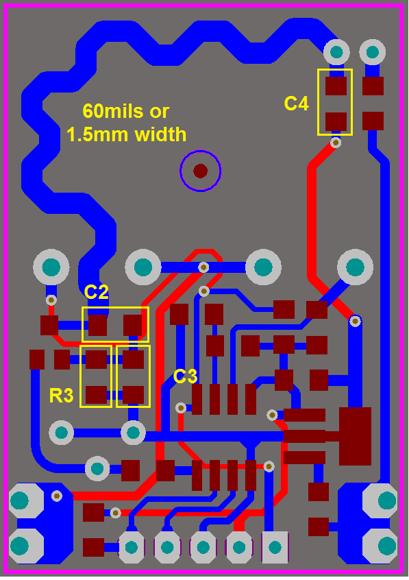
I'm running a simulation of your schematic. 1pF is a reasonable value for those capacitors. (5pF starts to create undesired waveforms.)
It looks as though your inductor is fabricated on the pcb. No value is stated. In my simulation a reasonable value for the inductor is 150-500 nH. This yields healthy voltage swings. Output at the collector leg is approximately a sine wave, min 0V, peak 21V.
Inductor value below 150nH generates irregular waveforms probably due to resonance with the capacitors.
C4 appears to have no useful purpose. As far as I can tell it drains away signal which is supposed to go to the amplifier.
C4 is necessary, it prevents the battery wiring influencing the antenna resonant frequency.
Brian.
I don't see how the PCB "antenna" structure can resonate at 434 MHz. Did you calculate the length?
If I remember correctly, the capacitors in a wireless doorbell transmitter with a similar antenna were 39pF which would make more sense than ~0.5pF to make it resonant. Unfortunately I don't have one to hand to check the values. I agree it probably resonates at much higher frequency at the moment, even if the resonator was for 866MHZ which they sometimes are. C4 is still necessary though to add bulk capacitance across the battery wiring.
Brian.
The circuit of RF and the antenna length/drawing were copied from a commercial board of a garage opener, this is why I didn't supplied its inductance value, and also I don't know how to measure it.
On original circuit, "RF-TX" signal (R1) was driven by a 0-12V digital signal, and in my circuit the same signal is driven by a 0-5V digital signal from MCU. Does this difference interfere on the transmission power? Could I reduce R1 to increase RF power?
I'm getting around 20 meters of range... a little less.
I have a logic analyzer connected at the output of the RF receiver. When I'm at a distance of around 20 meters of distance (transmitting constantly), the output signal get some glitches, undesired variations of logic levels which corrupt the reception of a data packet, that is around 80 bits using manchester encoding in my case. I will compare the output signal of receiver between my transmitter and the original transmitter tomorrow.
I corrected my simulation so C4 connects at the other end of the antenna. As Brian points out it has a useful purpose to stabilize the power supply.
Looking at your schematic I thought it resembles a type of Colpitts oscillator. So I assumed the antenna is an inductor. I guess I was mistaken because the SAW device is labelled 434 MHz. I'm not familiar with its workings but I suppose it has to do with modulating 434 MHz?
I once read an old-timer explaining how important it is to tune the output stage of a radio transmitter, so the antenna broadcasts at maximum strength. I believe the aim is to achieve resonating action, producing standing waves in the antenna so that it emits photons (electromagnetic waves).
It's worth a try since a 0v to 5v signal is able drive the transistor, yet it also needs to compete with the Saw device. if R1 is 5K then 5V applies 1mA, a reasonable amount.
R3 C3 are a normal rf amplification tactic used in the emitter leg. DC goes through R3 which turns on the transistor. C3 admits AC providing AC gain. To get more gain you can try reducing R3 and increasing C3.
In my own schematic and PCB, original values were: R1 = 47K, R3 = 150 Ohms 1%, C2 and C3 = 1pF
As suggested by BratheRad, I decreased R1 from 47K to 22K, decreased R3 from 150 Ohms 1% to 120 Ohms 1%, C2 = 1pF (no change) and increased C3 from 1pF to 1.5pF.
With these modifications, I got around 4~5 meters more in range. That's great.
From a distance from where the original schematic almost always failed, with the new schematic it almost always work.
Then I increased C3 again, to 2.2pF and, in my perception, the result was a little worse, but I don't have sure about that statement, it was just my impression, so I kept C3 as 1.5pF.
I was wondering if when increasing C3 to 2.2pF, if it's recommended to decrease R3 again, to 100 Ohms for instance. If yes, I'll do that modification on next week and test again. Or also, a combination of R3/C3 = 100R and 1.8pF...
Regards.
R3 should remain at around 120 - 150 Ohms, it is the capacitors and inductance of the track that make the big difference.
The resonance you are looking for for best range is set by the inductance of the loop and the three capacitors. C4 is large (and should be) compared to C2 and C3. You need to find the optimum values for C2 and C3 which should be approximately equal to each other. A small change in one capacitor such as 1.5pF to 2.2pF may slightly alter the resonant frequency and hence radiated power but my guess is they should be significantly larger. Try changing both to 3.3pF or 4.7pF and see what happens. Without knowing the inductance of the loop (and with a shape like that it would be difficult to work out) it isn't possible to calculate the exact values you need.
You could also try a capacitor directly across the loop, directly across the top of C2 to the top of C4 on the schematic. If you make a 'twist' capacitor you can easily experiment to see it if helps. Use about 15mm of thinly insulated wire for each side of the capacitor and twist them together, the tighter the twisting, the higher the capacitance will be. When you find the best 'twist', carefully unsolder the wires and measure the capacitance between them then use a fixed capacitor of the same value.
Brian.
With 120R and C2/C3 = 3.3pF the circuit does not work.
Until the previous post, the best results were with R3 = 120R, C2 = 1pF and C3 = 1.5pF. So I only changed R3 to 100R and got a little better result, but this improvement can be only an impression, I will keep R3 as 120R, C2 = 1pF, C3 = 1.5pF and R1 = 22K.
Brian, what is the name of the equipment suitable to measure the inductance of a track like that? Is it expensive? Could you recommends a model? I'm imagining an equipment with two probes connected at both ends of the antenna track (between the top of C2 and top of C4), applying a 434Mhz signal and measuring the inductance at this frequency. Is it something like that?
Regards.
It is very difficult to measure such a small inductance for several reasons:
1. the track is short compared to the wires connecting it to the inductance meter,
2. the substrate (PCB material) changes the inductance so you need to know it's parameters to factor them in.
It is probably easier to assume it is a straight length of copper track and calculate it from that. Capacitors are far easier to measure. I have quite a good selection of test equipment here but for most 'quick checks' I use one of these:
https://www.ebay.co.uk/itm/Mega328-L...UAAOSwM5tcTJug
It works surprisingly well and tests lots of other components too.
If you try the 'twist' capacitor trick you can carefully remove it from the board and measure its capacitance with a tester like that then fit one of the same value as a permanent replacement.
The better way to tune the circuit is with a GDO 'gate dip oscillator' which is basically a tunable oscillator with a frequency scale and a meter reading the current it is drawing. You place its coil near your circuit and adjust it's frequency until there is a change in current due to the transfer of energy between coils. Reading the GDO scale tells you the frequency your own circuit is resonant at.
Brian.
I will try the twist capacitor next week.
There's an university in my city, I can visit them, I think they have a RF/communications lab with some special equipments, maybe they have a device that can measure the inductance. What is the kind of special equipment that makes that measurements? Network analyzer?
PCB material is FR-4 (fiberglass) and will always be.
A network analyzer is better suited to situations where there is an input and an output to a circuit than a simple tuned circuit but it could be used.
A GDO is probably the best option, you don't actually need to know the inductance, only the frequency the tuned circuit resonates at. That frequency is primarily decided by the ring of capacitors around the inductor, C2, C3 and C4. Personally, I wouldn't get too deeply concerned about exact values unless you are mass producing these things, the twisted wire trick only takes a few minutes and is quite reliable.
Brian.
The transistor output capacitance is a relevant part of the total resonator capacitance, correct resonance measurements can be only made with applied CB bias voltage.
I believe the loop inductance can be better estimated than measured, I expect 50 to 60 nH. Due to the "antenna" being an electrical small loop, the most effective way to increase the radiated power apart from tuning the LC circuit to the transmission frequency is to increase the loop size.
I'm attaching some pictures: the current schematic (best results until now), Rev.A layout (current), and two possible future layouts Rev.B and C.
On next weeks I'll be producing a new prototype PCB panel from boards of other project and I can include 2 or 3 different layouts for that transmitter together in the same panel. I can test them and post the results here.
On all pictures, the track of the "antenna" have 1.5mm / 59 mils width, on a 1.6mm thickness FR4 board... the radius of the curves are 3mm in Rev.C.
On the pictures, between Rev. B and C, what is the 'best' drawing for an antenna? Does the shape influence on its behavior?
I already saw antennas with rev. C shape in some garage door openers.
I wonder if I can choose a specific shape, make the track with specific width and lenght (and maybe radius) to predict a good loop. Is that possible?
'doubling back' the trace so its direction reverses is usually a bad idea, at least on such a small board. There is a danger that the radiated EM field cancels itself and therefore has shorter range.
An open loop would be my choice but again I would tune it with a parallel capacitor to bring it into resonance. Note that it would be a good idea to flood fill all the PCB area, except under the antenna footprint, with ground. In particular you want the ground side of C4 to have as low an impedance as possible, at the moment your antenna track effectively extends through C4 and continues along the thin red track making it longer than you think.
Brian.
Brian, thanks for your help.
What do you want to mean with "open loop"? I think I understood what you said about 'flood fill' with ground. I can use a 'polygon pour' at the red/top layer of the PCB to have a lower impedance between the ground of the amplifier circuit and the ground connection of C4. Take a look, I did another antena track and the fill.
Which antenna drawing do you suggest for my case?
These are an actual 433MHz sender from a remote doorbell unit.
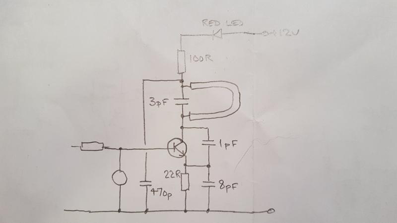
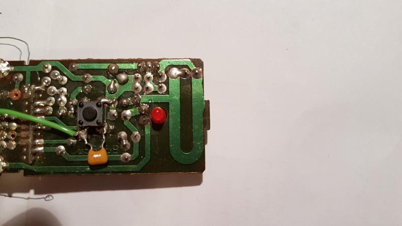
The transistor is an MPSH10 and the inductor dimensions are:
internal gap 3mm
track width 2.5mm
length from 3pF cap to outside tip of inductor 24mm
The 3pF capacitor is directly across the inductor ends.
Staying with your original layout - yes the 'polygon pour' looks good.
Brian.
Now looking at your schematic, I don't know what to do, because the circuit is a little different. Your schematic have a 3pF in parallel with the antenna. Mine schematic have C4 (470pF), one side of it is connected to the antenna but the other pin is connected to GND. I'm not understanding how can I implement the antenna shape of your doorbell in mine PCB, considering the last drawing I sent.
Also, it is unfortunate that I do not understand these types of circuits, how they oscillate, in detail, and what's the purpose of each component, mainly the SAW ressonator. I think I learned about these oscillator circuits about 10 years ago in communications lessons at the technical course, but I have never used them in practice and never had to calculate this kind of circuit, and I ended up forgetting.
But thanks anyway for your kindly help.
The circuit is identical except for the component values. The 3pF capacitor is equivalent to the 'twist' capacitor I mentioned before.
I would be inclined to use the design in post #17 but add the extra capacitor at the bottom left end of the antenna. Ideally, it should be directly across the two ends but with the ground plane (polygon pour) in place it should be safe to add it between the ground plane and transistor collector pin. The idea of C4 being 470pF isn't because that value is critical but that it has a high enough value to be seen as a short circuit to the signal at 433MHz. According to the XC formula, it has a reactance of only 0.78 Ohms at 433MHz! That means that the antenna is effectively grounded at one end and driven by the transistor at the other. Connecting the new capacitor from collector to ground plane is therefore electrically very similar to connecting it across the antenna ends.
The inductance on your design will be slightly different to the one in the photo but you can compensate for that by using a more appropriate value for the new capacitor. Again I would advise a twist capacitor to do experimentation for best range then measure and replace it with a fixed value afterwards.
The twist capacitor is VERY simple to make, just use two short wires, at least one of them insulted and twist them together. The tighter you twist them the higher the capacitance will be. Twist and untwist for best results then either leave it in place or swap for a fixed capacitor of the same value. If you use lacquered copper wire (as used in transformers) with a length of about 15mm you can create a variable capacitance from almost zero up to about 15pF.
Brian.
