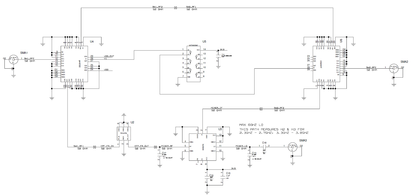
Switched harmonic test
Components used:
(a) Switches: Peregrine 42522
(b) Mixer: LTC5549 (with built-in LO frequency doubler) path measures H2 & H3 for 2.3GHz - 2.7GHz, 3.3GHz - 3.8GHz
(c) HFCN-4400+
(d) Southwest Microwave 292-06A-5
SMA Jack 50ohm edge mount
(d) Through path measures Power Out , ACLR, etc.
Q2-
May I know what is the difference between (a) Coated Microstrip & (b) Coated Coplanar Waveguide with Ground ?
Which to use ?
PCB material: RO4350 & 4403
Er: 3.5
No of PCB Layers: 4
Board thickness" 0.062"
Q3-
Is test coupon required
Is there a specific
I am a newbie to RF and was given a schematic to do pcb layout and simulation (cadence allegro & sigrity)
Schematic given:

Components used:
(a) Switches: Peregrine 42522
(b) Mixer: LTC5549 (with built-in LO frequency doubler) path measures H2 & H3 for 2.3GHz - 2.7GHz, 3.3GHz - 3.8GHz
(c) HFCN-4400+
(d) Southwest Microwave 292-06A-5 (SMA Jack 50ohm edge mount)
(e) Through path measures Power Out , ACLR, etc.
Downloaded each component reference design, ?cut & paste? and modify into one layout file.
SMA1 & SMA2 trace length 0.909?, trace width 0.025?, trace thickness 2.8oz, ground strip separation 0.008?

Some questions below:
1- Mixer LO max 6GHz.
For wavelength calculation, the frequency value is 6GHz ?
2- Is it true, RF trace length ideally should be less than 20mm.
Current trace length 0.909? (23mm)
3- SMA3 total trace length
(a) Does it need to match length with SMA1 & SMA2 0.909?
(b) Total trace length = Mixer U3.pin 11 to SMA3 ?
4- May I know what is the difference between (a) Coated Microstrip (b) Coated Coplanar Waveguide with Ground ? and which to use ?
Plan: PCB material RO4350 & 4403, Er: 3.5, 4 Layers, Board thickness 0.062"
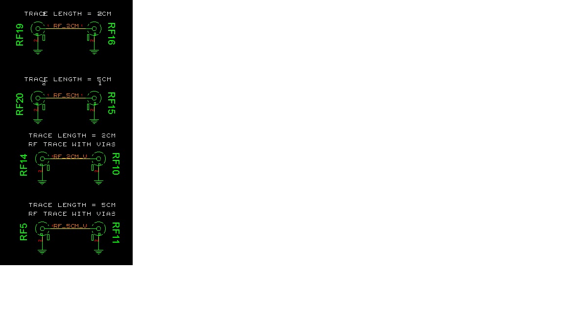
5- Saw some RF reference designs, there are something like test coupon with different trace length.
Need to implement ?

1- Microstrip & Coplanar Waveguide are different methods to draw traces in uWave frequencies; their difference is how they get the ground. Basicly speaking, microstrip gets the ground from the layer below; while CPW gets from both below and from sides. You should determine the trace width depending upon your carrier frequency. There are many sites/tools in internet that can help you with that. First step is to choose your Transmission line width for your carrier frequency using the substrate information.
2-4 Layer PCB design is quite hard if you have no previous experience; basicly speaking you use each layer for a different purpose. 1st one is for uWave traces, then for DC bias etc.
3- The mixer you wrote has an internal LO(Frequency generator ), it can either be used for upconversion or downconversion. When it say 6GHz, it means that you can get 6GHz at max from LO, depending on addition or substraction.
4- Generally speaking, the length of your trace changes the phase of your signal, so if you have a 2Ghz signal with 15cm wavelength; and a 3.75cm trace length in total; for a simple sine wave you go 1---->0.
Start with simple things, dont confuse yourself with details.
