how they simulate this 3 stages amplifier?
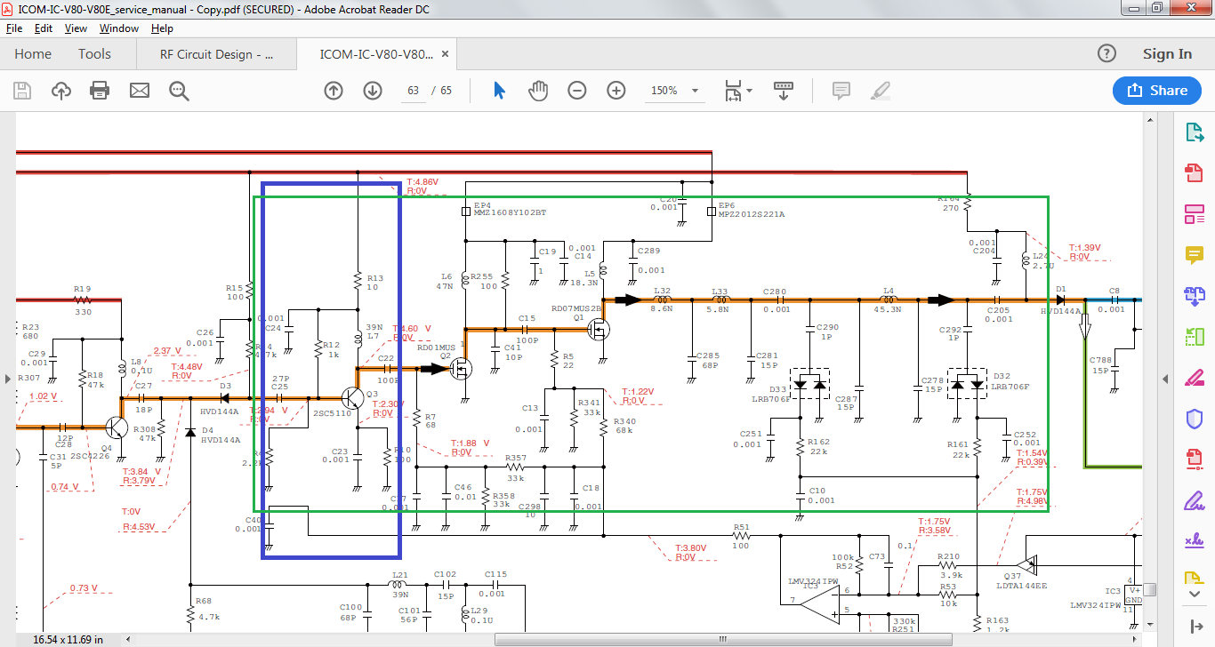
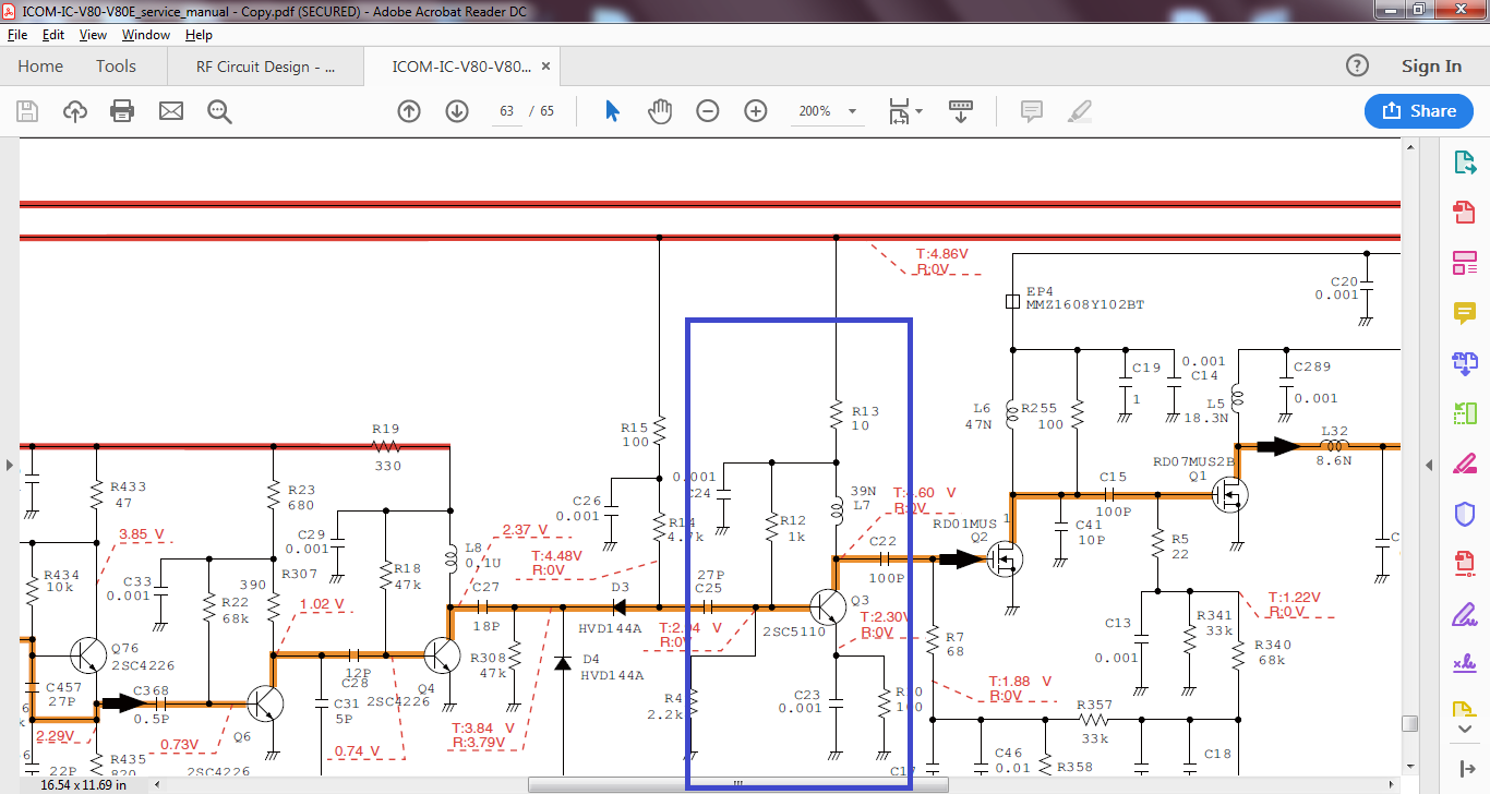
please any body can tell me how they simulate this (ICOM v80) 3 stages amplifier? and what is the suitable model they used?
thank you in advance!

Can we be certain whether it was drawn in a simulator? It has several markings and notations which suggest it was done in a drawing program for electronics.
In any case a simulator is able to calculate for 3 transistors/ mosfets the same way it does for one transistor. It may take longer to run since it is more complicated. And it's easy to make mistakes when drawing it, causing more errors. These have to be identified and corrected. And there are times you need to use a handy trick so the simulator doesn't hang.
thank you for replying.
it is practical schematic for ICOM v80 transceiver from it's service manual. not simulation circuit but i want to know if they simulate circuit like this, have they got close result in comparison to practical result?
if we talk about first stage, is it class a amplifier? has it impedance matching?
what is the model used for simulation this stage? is it Gummel?Poon model? is it another model can used for simulation like this class a amplifier?
what is the suitable model for using in calss a amplifier? and where can i find model for 2sc5110 BJT?
thank you in advance!

Q6 stage is a wideband amplifier and doesn't have a specific input/output matching network.
Q4 use L8 and C27 as output matching network, Q3 use L7 and C22 as output matching network, and Q2 (the driver stage) use L6 and C41 as output matching network.
The final stage Q1 use L5, L32, C285, L33, C281 as the output matching network.
The RF MOSFETs are from Mitsubishi and their models are available from Modelithics. Unfortunately not for free.
https://www.modelithics.com/model#mdlxcomp
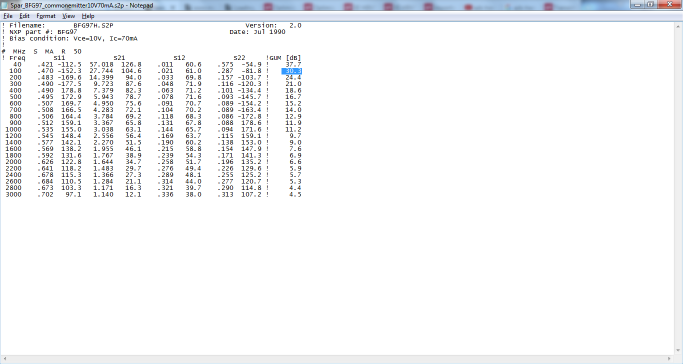
Inside of the 2SC5110 datasheet are available the small-signal S parameters. Starting with 200MHz up to 2GHz, but some simulators are able to extrapolate very well down to 144MHz.
http://radiocom.dn.ua/image/data/pdf/2SC5110_TOS.pdf
thank you so much vfone
i appreciate your effort for replying.
for Q4 why it dosn't has dc-block capacitor?
why we can't named c22 as dc-block capacitor for coupling two stages amplifier?
is there source explain how to design class a rf amplifier with impedance matching?
thank you in advance!
You may name C22 a DC block capacitor.
There are a lot of papers and books available on the net for PA impedance matching. Just search for them.
http://mwl.diet.uniroma1.it/people/p...Amplifiers.pdf
The reactance matters. 1 nF (X ≈ 1 ohm) can be considered as pure DC blocking capacitor, 100 pF (X ≈ 10 ohm) is already modifying the impedance.
thank you so much vfone
there is no problem for designing impedance matching.
my only problem is how to make class a circuit amplifier simulation in ADS for getting (30.3 dB) gain @ 100 MHz and (24.4 dB) @ 300MHz like result from s2p for bfg97 bjt ?
thank you in advance!

no body can make real simulation for rf amplifier to get real result as same as s2p file?
anyway thank you
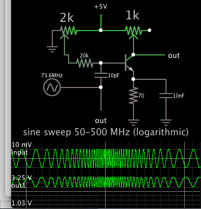
The common emitter arrangement is typical in a Class A amplifier. In case a simulation will help, here is a basic amplifier providing over 200 gain.

Frequency sweep is 50-500 MHz. Component values were found by experimentation, with the aim that they amplify those frequencies.
