design and simulation of cross-coupled VCO using keysight ADS
I am currently working on designing a low-power consumption and low phase noise cross-coupled VCO in keysight ADS. I am not getting the transient response i.e the oscillating waveform for my circuit. Could anyone please guide me through the process. I am hereby attaching my design for the reference.
You connected the base of each BJT transistor directly to the other BJT collector, which is wrong.
The DC bias of the cross-coupled VCO should look as in the schematic below:
https://www.researchgate.net/profile...-schematic.png
-OSC_PORT is wrong placed, you cannot obtain any result from it..You must cut the feedback path and place it there..
-In order to get a transient simulation you have to excite the circuit temporarily to make it leave from initial condition.
-There is a good circuit in ADS examples ( keyword: CMOS VCO) , open it and inspire how a simulation setup has been prepared.
To start your circuit oscillating, it helps if there is non-symmetry between the left and right half.
This simulation seems to work okay.
The waveforms show that current flows back and forth in a loop formed by L1 L2 and the capacitor. If the capacitor is omitted then a different mode of operation takes place, namely the left half conducts while the right half is off, then its vice-versa.
I just found that your DC supply (V_DC) is placed in reverse position.
If use NPN BJTs, the negative (-) shall be connected to the ground, and positive (+) to the transistor collectors.
Hi. thankyou for your reply. Could you please tell me how to excite the circuit temporarily and also there is no relevant example on cross-coupled VCO in ADS. If possible can be please provide me with the details. Thanks in advance.
Create an imbalance somewhere, to cause either the left or right half to conduct more than the other.
Possibilities:
* Make one inductor value different from the other.
* Assign a charge on the capacitor starting at t=0.
* Provide any node with a momentary connection to a supply rail
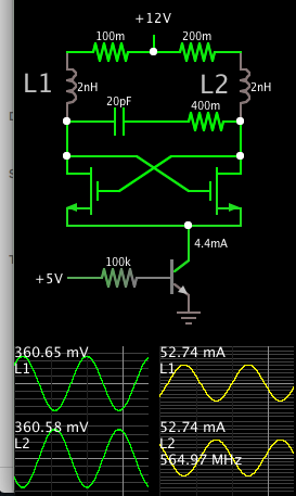
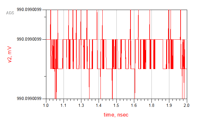
Hi. I have used a small signal model instead of actual transistor just to check whether I am getting an oscillating waveform in trnsient response. But I am getting the results as follows. Can anyone please help me regarding the issue.
[Found at imgur. com /a /18smyoP]
Hi. I am designing a cross-soupled VCO in ADS. The circuit diagram using the small signal model of transistor is as follows. While performing the transient simulation, I am not getting the oscillating waveform. Can Anyone please help me out with the issue. Thanks in advance.
https://imgur.com/a/18smyoP
Small signal Models are NOT used neither in Transient nor HB analysis.
You have to read "fundamentals of simulation techniques" from different tutorials/app. notes.