Half-mode SIW Simulation
I am having a problem on simulating a half-mode SIW in HFSS.
Since we cut the width by half, the resulting structure has cut-off frequency double the original one.
But all papers said they have very close responses.
Any idea how should I simulate the half-mode structure?
Thank you for your help!
hello, the em fields are similar to that in HF siw. If you cut the siw into two identical ones, the fields almost have no change if w/h is very large.
Could you post an image of your model? You probably have conducting wall on the plane of cut, so it halves waveguide width and doubles frequency. In this case solution would be removing conductive wall on that side.
Thanks for your answers!
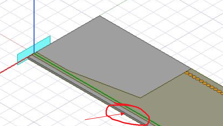
Please see two images of the structure
Could you please tell me how to do it?
Thank you for your help!
I am not familiar with HFSS, just guessing from your image: check this vertical thin wall is not conductor, ensure there are no any hidden walls inside substrate on this side:

What is outer material on this wall? PML? or maybe HFSS puts PEC (conductor) by default?
This wall is the substrate, no conductor here except at the bottom of the wall, there is a bottom horizontal ground (which is a conductor).
I didn't define any boundaries or excitations to this wall. I tried to draw a vertical rectangle there and define it as "perfect H" and "symmetry perfect H" but the responses were almost the same.
Based on papers, the high ration of w/h will act as a PMC by default.
You may try this:
1. extend dielectric substrate on this wall (near Y axis), only conductor is cut but not dielectric.
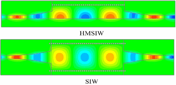
2. check EM-fields distribution in HFSS, result must look similar to this image:

(image from Yuanqing Wang, Wei Hong "Half Mode Substrate Integrated Waveguide (HMSIW) Bandpass Filter")
As you can see those field distribution "blobs" are cut by half. If they are stretched along Y axis, then boundary is wrong.
We need someone who familiar with HFSS. It is unclear how top and bottom surfaces of substrate are handled, what boundaries are put by HFSS for this model. EM-filed distribution image may help to understand this problem.
Can you please show us:
The fields of the mode(s) you are exciting.
The surrounding radiation box (extent of the simulation domain).
Thank you.
The setup and solution appear to be correct -- so what is the issue, exactly?
Can you plot the S-parameters of this setup and that of a similar full-mode SIW?
Thank you for your feedback.
Here are the S-parameters of the full-mode SIW (calculated at 50 ohms port impedance) using two different tapered widths.
Next, S-parameters for the HMSIW
My main problem is that when I simulated these two structures without the tapered microstrip feedlines, the cut-off frequency will be doubled!
But as you can see in Fig. 7 in the paper below, it should be the same.
http://http://citeseerx.ist.psu.edu/viewdoc/download?doi=10.1.1.728.5011&rep=rep1&type=pdf
They look to be about the same (cutoff around 5 GHz).
So you showed us the simulations that worked, but not the ones that didn't work. How are we supposed to help you? Please show us the same data and figures for the cases that didn't work as you expected.
Thank you for your reply.
Here is the structures and S-parameters as well as to beta (which shows the cut-off frequency) of the Half-mode and full-mode structures.
Full-mode:
Half-mode:
Alright, so your half-mode data is not self-consistent: the S-parameters clearly indicate that the cutoff frequency is around 5 GHz, but the Beta plot is showing that you have a cutoff around 10 GHz.
Quite possibly it's a simulation error in the wave port: sometimes they will solve for one mode at the convergence frequency, but another will be excited in your frequency sweep. What is your simulation setup (convergence frequencies, etc.)?
Could you please show the port fields on both ports at 5.8 GHz and 11 GHz. Alternatively, upload the HFSS file and I can take a look at it.
Thank you very much for your help.
Please find attached the HFSS files of the half-mode and full-mode structures.
SIW.rar
From S-plot it is obvious that cutoff is around 5GHz, but it is not matched. Your Half-mode SIW S-plot shows big insertion loss around 5GHz. Probably placing waveguide port directly on HMSIW edge results in big mismatch, because port width is halved, but "magnetic wall" and symmetry does not act for port the same way as for waveguide. Solution would be to change something in port configuration, or to use transition as in your earlier post.

Ok, so look at this figure. Your port is exciting a full mode in the HM-SIW, which is why it shows cutoff around 10 GHz.
There's not an obvious reason why this is happening, it's just HFSS not getting the correct mode. You can probably resolve this by changing the convergence frequency (you have it at 6 GHz, I'd set it lower to about 4).
Also, the port won't include fringing fields coming out of the HM open edge. I'd recommend enlarging your port such that it encompasses more of the modal fields.
Indeed, this is why HFSS introduced "symmetry boundaries", which are just perfect E/H, but also modify port impedance.
