Re: microstrip low pass filter design issues with sonnet

Someone told me the above with regards to the two extra rectangles nearest to the ports.
What do you guys think ?
What about in HFSS ?
Z0 is related to the line cross section. For a lossless line it is sqrt(L'/C') where L' is inductance per unit length and C' is capacitance per unit length. So you can see that line impedance itself does not depend on the line.
A coax line of 50 Ohm remains a 50 ohm line, no matter if you cut it into pieces of 1 meter or 1 inch.
But don't confuse that with the effect of impedance transformation caused by a line - that of course depends on line impedance and length.
~~
Just in general, we add 50 Ohm line as interconnect between RF blocks for purely practical reasons (keep blocks in layout at reasonable distance). There is no special RF effect or purpose, it's just an interconnect, with no impedance transformation. That's the special case: if source impedance = load impedance = line impedance = 50 Ohm, we have 50 Ohm at the input and output of the line, no matter what the line length is.
Yes, Sonnet can remove the effect of the feedline at the port if reference plane shift is used. Sonnet then calculates the line properties and removes them from the total result.
That reference shift is then visible in the Sonnet editor, by arrows from the port up to the reference plane.
This is useful if you want to have the S-parameters of the "inner" device without feed lines, but need to add some lines to keep that inner device away from the Sonnet box walls (metal).
~~
I think you have to think (or read) about all this transmission line stuff to connect some more pieces of the puzzle. It's not that complicated, but you seem confused what lines are meant as simple interconnect (50 Ohm) and what have a special purpose (impedance transformation where Zload is different from Zline).
What do you exactly mean by reference plane shift ?
http://www.sonnetsoftware.com/suppor...embedding_.htm
http://www.sonnetsoftware.com/suppor...d_feedline.htm
I have inserted the feedline as shown in the figure below. May I know how to generate a DXF layout file (without the extra feedline structure) for actual manufacturing purpose ?
By the way, is FR-4 with height 1.6mm and Erel of 4.2 common for chinese PCB manufacturers ?

three-pole microstrip lowpass filter using open-circuited stub.son
FTYP SONPROJ 13 ! Sonnet Project File
VER 15.53
DIM
ANG DEG
CAP PF
CON /OH
FREQ GHZ
IND NH
LNG MM
RES OH
END DIM
FREQ
ABS_ENTRY 0.001 6.0
END FREQ
CONTROL
STD
OPTIONS  -bdj
SPEED 0
CACHE_ABS 1
TARG_ABS 300
Q_ACC N
END CONTROL
GEO
DRP1 LEFT LINK
POLY 13 1
0
DRP1 RIGHT LINK
POLY 15 1
0
TMET "Lossless" 0 SUP 0 0 0 0
BMET "Lossless" 0 SUP 0 0 0 0
MET "Copper" 1 NOR 58000000 1 0.01
BOX 1 36.1 12 722 240 20 0
      20 1 1 0 0 0 0 "Air"
      1.6 4.2 1 0.02 0 0 0 "FR-4"
LORGN 0 12 U
POR1 STD
POLY 13 1
2
1 50 0 0 0 0 8.78975
POR1 STD
POLY 15 1
2
2 50 0 0 0 36.1 8.790025
NUM 5
0 5 -1 N 11 1 1 100 100 0 0 0 Y
5.010005 8.689745
16.050005 8.689745
16.050005 8.889745
5.010005 8.889745
5.010005 8.689745
END
0 5 -1 N 12 1 1 100 100 0 0 0 Y
20.049995 8.690025
31.089995 8.690025
31.089995 8.890025
20.049995 8.890025
20.049995 8.690025
END
0 5 -1 N 13 1 1 100 100 0 0 0 Y
5.01 9.38975
5.01 8.18975
0 8.18975
0 9.38975
5.01 9.38975
END
0 5 -1 N 15 1 1 100 100 0 0 0 Y
31.09 8.19003
31.09 9.39002
36.1 9.39002
36.1 8.19003
31.09 8.19003
END
0 5 -1 N 17 1 1 100 100 0 0 0 Y
16.050005 3.109975
20.050005 3.109975
20.050005 8.889975
16.050005 8.889975
16.050005 3.109975
END
END GEO
OPT
MAX 100
VARS
END
END OPT
VARSWP
END VARSWP
QSG
IMPORT NO
EXTRA_METAL NO
UNITS YES
ALIGN NO
REF NO
VIEW_RES YES
METALS YES
USED NO
END QSG
TRANSLATOR
DXFEXPORT
UseTLs false
SepObj true
SepMat true
DivideMulti false
Circles false
CircleType inscribed
CircleSize 0
KeepMetals true
KeepVias true
KeepViaPads true
KeepBricks true
KeepEdgeVias true
KeepParent true
ConvertParent false
AllEdgeViasAsVia false
END
END TRANSLATOR
If you have a license for Sonnet DXF option: File > Export > DXF
will export the layout "as is", including those feedline.
On PCB, you will need some length of 50 Ohm line to attach the connectors. The narrow (inductive) lines are most likely too thin to solder the connectors. And let me repeat: if the extra line is 50 Ohm (which I haven't checked) then it doesn't change your filter response (magnitude). It only adds some delay (phase).
If you insist to export a different version of the layout (excluding the 50 Ohm lines), create a copy of the file and modify the layout.
Yes, those are typical values. Specify the correct thickness.
And make sure your layout includes bottom ground also. In Sonnet, you didn't draw that because the bottom of the Sonnet box is metal boundary. For your PCB order, you need to include that backside ground metal in your files. One possibility: You can draw a polygon on the Sonnet ground layer. This has no effect for Sonnet, but will be included in export.
I have added a polygon covering the entire box region at the GROUND layer.
However, I am not sure if I have actually added a ground metal plane.
I could not see the ground plane using 3D viewer of Kicad PCBNew software.
Could you advise ?
Note: I have attached the dxf layout file as a zip file at the end of this post.


three-pole microstrip lowpass filter using open-circuited stub.son
FTYP SONPROJ 13 ! Sonnet Project File
VER 15.53
DIM
ANG DEG
CAP PF
CON /OH
FREQ GHZ
IND NH
LNG MM
RES OH
END DIM
FREQ
ABS_ENTRY 0.001 6.0
END FREQ
CONTROL
STD
OPTIONS  -bdj
SPEED 0
CACHE_ABS 1
TARG_ABS 300
Q_ACC N
END CONTROL
GEO
DRP1 LEFT LINK
POLY 13 1
0
DRP1 RIGHT LINK
POLY 15 1
0
TMET "Lossless" 0 SUP 0 0 0 0
BMET "Lossless" 0 SUP 0 0 0 0
MET "Copper" 1 NOR 58000000 1 0.01
BOX 1 36.1 12 722 240 20 0
      20 1 1 0 0 0 0 "Air"
      1.6 4.2 1 0.02 0 0 0 "FR-4"
LORGN 0 12 U
POR1 STD
POLY 13 1
2
1 50 0 0 0 0 8.28975
POR1 STD
POLY 15 1
2
2 50 0 0 0 36.1 8.290025
NUM 6
0 5 -1 N 11 1 1 100 100 0 0 0 Y
5.010005 8.189745
16.050005 8.189745
16.050005 8.389745
5.010005 8.389745
5.010005 8.189745
END
0 5 -1 N 12 1 1 100 100 0 0 0 Y
20.049995 8.190025
31.089995 8.190025
31.089995 8.390025
20.049995 8.390025
20.049995 8.190025
END
0 5 -1 N 13 1 1 100 100 0 0 0 Y
5.01 9.88977
5.01 6.68973
0 6.68973
0 9.88977
5.01 9.88977
END
0 5 -1 N 15 1 1 100 100 0 0 0 Y
31.09 6.69002
31.09 9.89003
36.1 9.89003
36.1 6.69002
31.09 6.69002
END
0 5 -1 N 17 1 1 100 100 0 0 0 Y
16.050005 2.609975
20.050005 2.609975
20.050005 8.389975
16.050005 8.389975
16.050005 2.609975
END
1 5 -1 N 46 1 1 100 100 0 0 0 Y
0 0
36.1 0
36.1 12
0 12
0 0
END
END GEO
OPT
MAX 100
VARS
END
END OPT
VARSWP
END VARSWP
QSG
IMPORT NO
EXTRA_METAL NO
UNITS YES
ALIGN NO
REF NO
VIEW_RES YES
METALS YES
USED NO
END QSG
TRANSLATOR
DXFEXPORT
UseTLs false
SepObj true
SepMat true
DivideMulti false
Circles false
CircleType inscribed
CircleSize 0
KeepMetals true
KeepVias true
KeepViaPads true
KeepBricks true
KeepEdgeVias true
KeepParent true
ConvertParent false
AllEdgeViasAsVia false
END
END TRANSLATOR
I'm sure you'll figure it out ... just look at imported layers one at a time.
The DXF file created by Sonnet is 2D data, so don't expect different z position of signal and ground layer.
~~
You seem to be changing the width of the feedline again and again ... make sure the width is designed for 50 Ohm. I didn't check your files, only looked at the screenshots.
See https://github.com/promach/low_pass_filter
By the way, what is the difference between open-circuited stub and stepped-impedance ?
See 2GHz Microstrip Low Pass Filter Design with Open-Circuited Stub
I am trying to understand why open-circuited stub has a better S21 response compared to stepped impedance according to the result at figure 5.4 below:
this microstrip equation for Zo does not depend on length.
Could anyone point me to a microstrip equation that describes the relationship between stub length (in this case, 5.78mm) and λ/4 at 5.6 GHz and substrate properties (dielectric constant and thickness) ?

You implement that shunt C by a transmission line, and have some freedom in choosing a width and then calculating the required length. It seems that the "open circuited stub" layout used a length of lambda/4 at 5.6 GHz, so that the open end transforms into a short at that frequency, creating a notch at 5.6GHz.
Is it possible to prove this mathematically using some microstrip expressions ?
Yes, using the equation that gives input impedance as a function of line impedance, line length and load impedance.
This is not specific to microstrip lines.
Page 3, chapter "Impedance transformation"
http://muehlhaus.com/wp-content/uplo...sion-Lines.pdf
Someone else told me the above.
What do you think ?
Correct, my statement refers to lambda/4 effective wavelength (90° S21 phase) for the actual substrate.
Edit: Doing the math with the limited information that you supplied the S21 phase that I get is more like ~120° using ADS Linecalc, but the stub is rather wide and it gets a bit fuzzy due to parasitics. The math for notch length would be exact if you do circuit simulation with ideal elements. For actual layout, I guess length was adjusted to move the notch as required.
Could you post the ADS linecalc window screenshot which shows 120° ?
Here it is, with 1.27mm thickness at er=10.8 we get 115 degree
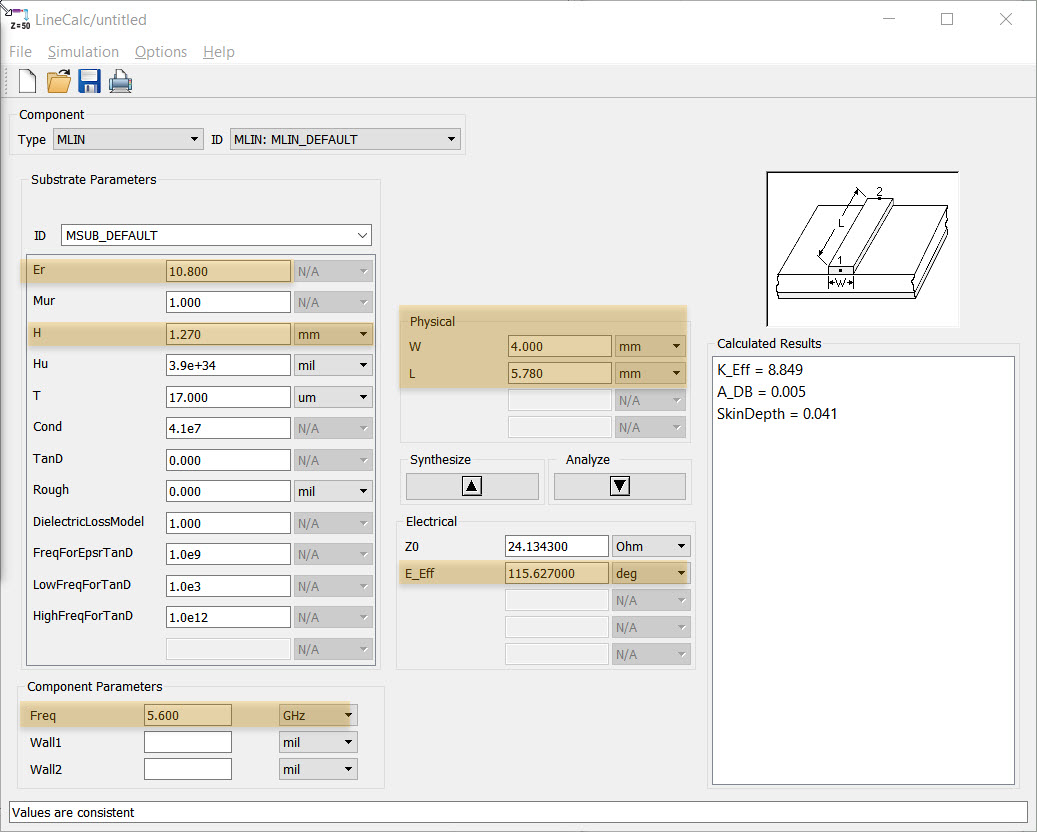
but that assumes a thru line. Due to the parasitics of an open ended line and the narrow feed from the side, we actually get the notch at 5.8 GHz.
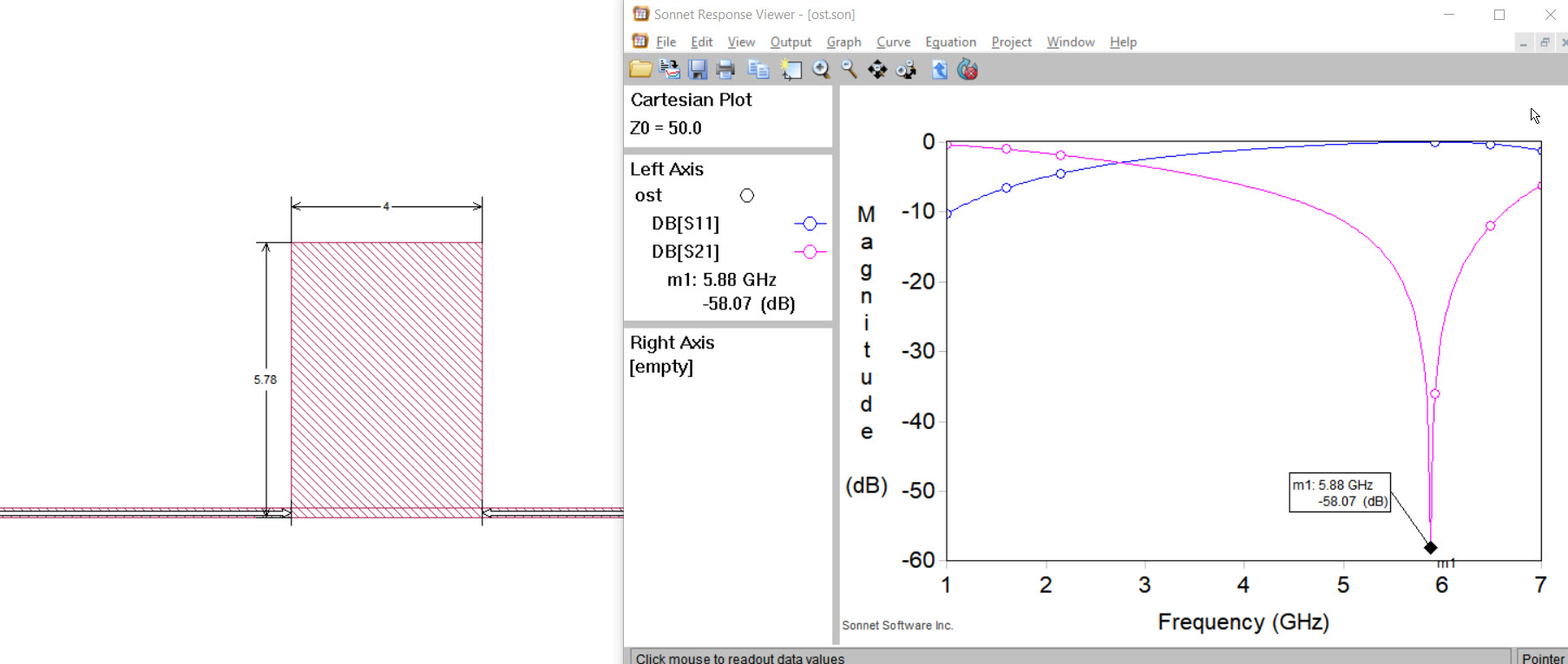
This is what we get in Sonnet for the open ended line, feed with 200μm wide strips, reference plane at the open stub (feedline not included in results):
Zipped Sonnet model: ost_model.zip