Positive S11 Parameter - Sample HFSS file uploaded
By the way, in this simulation, I'm trying to use glass to "shield" the RFID UHF tag antenna from the negative effects of the metal plate (simulated license plate).
Thanks!
hi
i cant understand what u want to ask and whats your problem
Well... If you "analyze" that file and look at the resulting S11 parameters, there will be a frequency that will have a positive value. I'll upload it here:
yes i saw it whats your problem with it,it like to appear upper than zero
my dear its a software and solve problem by numerical method so it common
Do you do a complex renormalization of the S-Parameter?
Then a S-parameter above zero could happen.
How do I NOT do a complex renormalization?... What setting do I change?
hi
if u choose active S it may vanish
Oh flip, all I needed to do was to choose active S and then dB10/dB20normalize. But what's the difference between the dB10normalize and dB20normalize functions?
Normally S-parameter are calculated for a 50 Ohm line resistance. But you could calculate for a complex impedance for example (50+j50) Ohm, then you could get S-parameter above zero.
The S-parameter is a unit less value, for better handling it is often stated in dB: S11[dB] = 20*log(s11).
I think die dB20 calculates it with the factor of 20, and the dB10 with a factor of 10 instead of the 20.
Thaaaaaaaaaaaank youuuuuuuuu everyoooooooone! =d
Hello all,
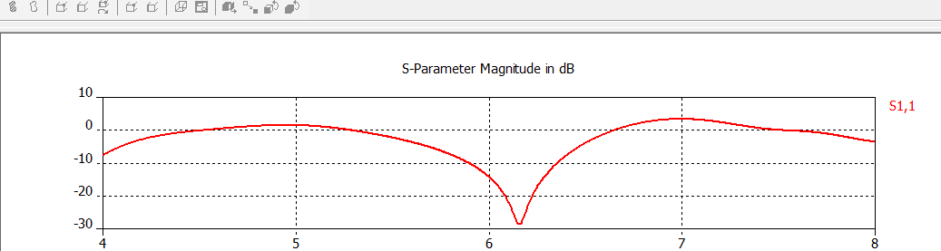
actually i am facing the same problem but with CST,the both side of S11 more than 0dB.
Is there anybody could help me please about this matter ?
i attached an image show the problem.
Appreciated
While I haven't done that before, it doesn't seem like that would solve your problem - it would give realistic values, but it seems like the values would still be warped due to the error introduced.
I've found that such behavior generally occurs for port heights of approximately lambda/2.
hi PlanarMetamaterials ,
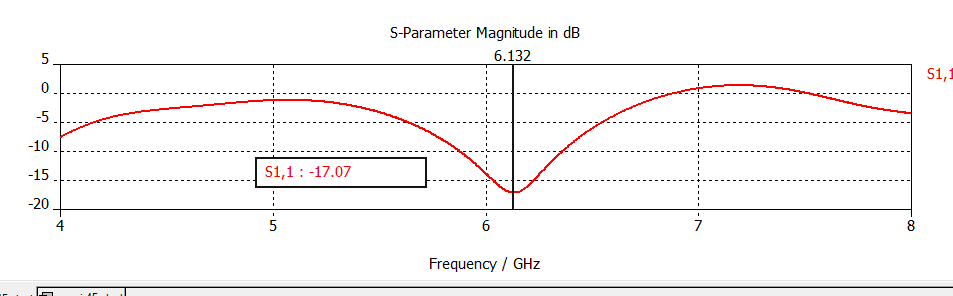
thanks for ur help, actually i changed the dimensions of the port and i reduced it's height, but S11 became like in the pic below!
i think it's much better but still there are frequencies have a positive value,
wt"s ur suggestions?
regards
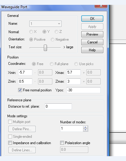
Huh, I'm not sure. What are your port settings?
- - - Updated - - -
the port size is 6 times as wide as the width of the microstrip line(1.9) and 5 times as high as height of the substrate(0.813),but when i use this height i got positive S11 in both side,and when i change it i get different result like the one i sent it to u before .
Have you looked at the mode it's producing? Maybe something strange is going on there. Also, maybe try defining the integration line manually.
You can try to improve the mesh or a larger frequency range.
hello all,
thanks for ur reply,
PlanarMetamaterials please,how can i define the integration line manually?
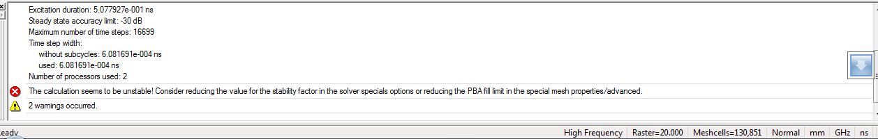
flanello i tried several times to change the frequency range and make it larger but it gives me error on the simulation((the calculation seems to be unstable!))
And what about the mesh?