How to simulate PIN diode in CST MWS with both OFF and ON states
i'm need to simulate a PIN diode in CST Microwave studio with both OFF and ON states and it needs to be reprensated as a lumped element with RLC values. I need those values to be accurate so the PIN diode model would be more realistic and the simulation more precise. I'm modeling an reconfigurabile patch antenna with an inset in which the diode would be mounted. So, basically, what i need is the values of R,L and C for the ON and the OFF state or/and some literature in which i can find those.
Thank you very much in advance..
The RLC values for the PIN diode model are going to a) be frequency dependant, and b) depend entirely upon the diode you're using!
The manufacturer's datasheet would be the first place to look - and if they don't specify what you need, go solder one across an SMA connector and plug it into the network analyser... (with appropriate bias) :)
hi, thanx for your answer, but can i ask for some more help..i can't find my way arround those parameters needed by cst mws. it needs: R-resistance, C-capacitance, Gs-conductivity when blocking, I0-reverse current and the datasheets of the diodes that i've found offer other parameters. e.g. reverse voltage, forward current, or R/C at lower frequencies that i need.
can you maybe suggest some "default" diode that has the parameters defined or at least point me to some relevant equations so i could calculate the needed parameters? thanx in advance
I never cease to be amazed at just how comprehensively everything is modelled in CST :)
If you are only going to bias the diode ON or OFF (and not try and use it as a non-linear device), you could try describing it as a lumped RLC component instead of a "diode". Then, all we need to do is arrive at sensible values for these three parameters for each of its two states. I'd anticipate the accuracy of this approach to be more than sufficient for most practical applications.
(Now, I'm making this up as I think on the fly, so feel free to suggest other possibilities!) - but in the ON state, I'd expect you could well describe the diode as a Z = series RL device, where R is equal to the diode resistance at the specific bias current used + a dynamic resistance (which increases with frequency) component. R = a few ohms would seem plausible. L will be dominated by the package parasitics - perhaps 0.1 -~ 2 nH?
In the OFF state, the low value R component will become much larger, to the extent I'd expect the impedance to be dominated by the (parallel) junction capacitance. (Apparently) the junction capacitance of a reverse biassed PIN junction is a) lower and b) less bias-dependant than the typical varactor-type bahaviour observed with the PN junction. As such, Z = a series LC, where L is the same as the previous case, and C = the junction capacitance. (~0.1 - 2 pF?)
You could then simulate both the ON and OFF states by performing a 2 point parameter sweep of R, L & C (where the start and finish values are their ON and OFF values) and picking the appropriate two (of the 6 total) result curves.
Hope that helps :)
Like thylacine1975, I would suggest to avoid the nonlinear diode model.
If you want to use the nonlinear diode model, your amplitudes and waveforms must agree with the amplitude and waveforms in the hardware. This makes your simulation more difficult, and does not add any value to it. Keep simulating linear, and model the diode with ON and OFF states equivalent circuits.
thx for the posts. @thylacine: indeed, my mentor did mention to use an RLC combination for the diode but i was unable to find those parameters at first, cause i was trying to find a straithforward solution. ok, i'll try to use your suggested values and see what the simulation will show, i also believe it will be accurate enough for my need. only, is there any formula i can use to calculate the R component when diode is in OFF state or should i just put some random value?
btw, i encountered another problem, this one with the model itself. the erorr that mws gives is: "the lumped element is inside perfect conducting material" and then stoppes the simulation. it seems (at least i think) that the mesh grid isn't thick enough to analyze the lumped element so i tryed raising the number of mesh cells but it didn't help. any advice?
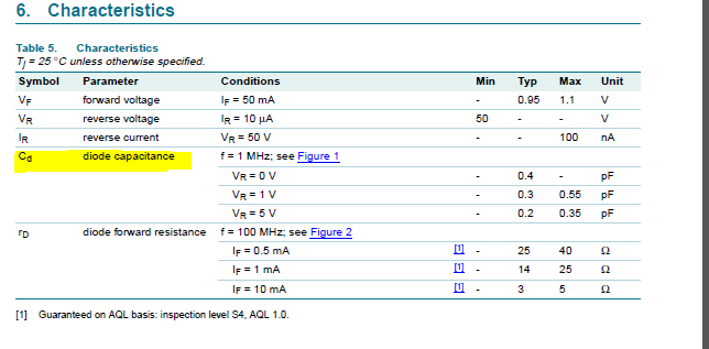
In OFF state, you can approximate you PIN diode with a capacitance. The value can be found in the data sheet for different reverse voltages.
Example:

ok thanx. let me just see if i got this right (i obviouslly should have studied more about pin diodes, sorry):
ON state - RLC serial combination where R is a few ohms (e.g. 5), C = 0 and L is 0.1 -~ 2 nH?
OFF state - RLC parallel combination where R = 0? and L is 0.1 -~2 nH and C as suggested, around 0.2-0.4 pF?
is that ok or have i missed something?
edit: just to let you know, about the erorr mentioned in my previous post, i've managed to solve it. it was caused by wrong z coordinates so the element was literally in the substrate layer. when i moved the element "up" to contact only the patch surface, the simulation worked ok. now i'll test the discused values..
No C. Use just R-L series.
No R. Use just L-C series.
but, that's exactly what i did. in the first case i defined C with zero value and in the second the R is zero valued -because of cst i have to put some value. as explained in cst help, when a value of any component is zero it simply removes it. i was just checking if the combinations were right: in the first case is a SERIAL R-L and in the second is the PARALLEL L-C, right? i'll assume that it is because you didn't correct me for that matter :)
For ON, you wrote serial RLC with C=0, which is wrong. If anything, you need a really large C value, so that the C is effectively a through connection at all frequencies.
For OFF, you wrote parallel RLC with R=0, which is wrong. You need C, or series LC.
now you've got me confused.
i wrote RLC series because it's the only option in mws, it has RLC serial, RLC parallel and diode, there is no options for only R-L or only L-C, but this is from the mws help: so, what am i missing here? can you tell me your solution to this problem? thanx
Sorry for that. Indeed, the text from the CST help is clear, although surprising.
In this case, use serial RLC for both ON and OFF. Why series? There is always some parasitic series inductance. In the ON state, it is in series with the ON resistance. In OFF state, it is in series with the OFF capacitance.
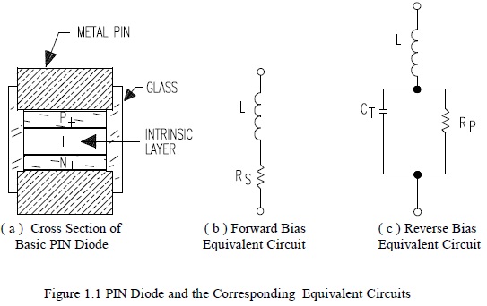
yes, it is a bit weird, but the again it is logical, because otherwise it would be impossible to simulate combinations other then R-L-C. btw, i've found the equivalent schemes for the pin diode

hopefully that will an adequate solution for my purpose.
hi guys, i've found and discussed with my mentor some values for the pin diode and decided to use these: for forward bias - R=3.5 ohm, L=0.45 nH; for reverse bias - R=3 kohm, L=0.45 nH and C=0.08 pF.
now, when i enter this in my model and run the simulation (in forward bias mode) i get the warning message: "the intrinsic cell inductance 8.885e-010H of lumped element PIN is greater than the defined parameter. please consider a mesh refinment at this location."
ok so i understand what the message means but i want to know does it affect the accuracy of the results? how can i avoid it without changing the value of L? and can you please how do i "refine the mesh at that location" because i didn't find the option to do just that. thanx again
I'm hoping someone will tell me this is the wrong way to do it and I'll learn something - I have often wanted to know how to do exactly the same thing!
But until then, what has worked for me is to globally increase the mesh density for the component(s) in question. You do this by:

...which forces the mesh to be finer than the specified maximum x,y,z steps. Unfortunately this sort of defeats the "intelligent meshing' algorithms which try to keep the calculation time down to reasonable limits and the problem tends to bloat computationally. If you were so inclined, you could note the number of meshcells reported at the lower right of the screen and iteratively fiddle the x,y,z step values to achieve the desired precision/calculation time. I just tend to set values which I feel "safely" quantize the mechanical features of the structure and leave it chugging while I go home and sleep :) An "increase mesh density by a factor of two" type button would be really handy!
Let us know how you go...
hi thylacine, thanx for your answer, i didn't have time to test your solution until today. so, i've tryed setting the simulation as shown on your screenshot and putting those three values up to 50 with no change in the warning message. also i have tryed setting the local mesh for only the patch not for all components and still nothing. i've tryed raising the global mesh lines per wavelength up to 20 and that didn't help either. i'm out of ideas, and the internet isn't very helpful regarding this topic. any other ideas?
Ah! Try setting them in the *opposite* direction - i.e. tiny... values like 0.1 or 0.01 or ...
These correspond to the maximum *physical* spacing (in mm, or whatever unit your CST environment is configured for) of the mesh cells. Start with something like the wavelength (of the highest simulation frequency)/20 and go down from there.
i was very busy this whole week so i couldn't answer until now. i have tryed what you suggested and set the values to 0.03, then 0.1, 0.5, 0.8 and the warning message was still there for all the set values, only the simulation time was shorter as i set the larger values. for the first two values (0.03, 0.1) i didn't even wait for the whole simulation to finish cause i would have taken approximately forever. i've tryed searching online for this warning but found nothing relevant. i don't know what else to try but to ignore it. only, i don't know in what measure it affects the accuracy of the simulation. maybe some other suggestion to try?
hi all, sorry to bump an old topic but i still haven't figured out the whole solution for the simulation with the pin diode. so, i configured it as an RLC serial component with the values as posted above. the problem that i'm having is that the software behaves as though the diode isn't even there. when i check the surface current view it shows that there is no current going through the diode in both ON and OFF states. so what am i missing? what else can i try to get this simulation working? thanx for any help provided.
- Using a diode connected transistor model in CST 3D simulation
- Rad. of Patch integrated with Diode switch and other lumped components in ADS & EMPro
- Modelling Schottky diode SMS-7630 in ADS for rectifier applications at 5.8 GHz
- Varactor diode tuning
- IR LED sensor in one Diode?
- Need suggestion on TVS Diodes DO-160 Lightning Protection
