Slotline Simulation in Ansys HFSS
时间:03-30
整理:3721RD
点击:
Dear all,
as I am having some trouble with my antenna design, I started splitting it up in small problems:
My very first problem is about designing a slot line and determining it's characteristic impedance Z_0.
My simulation is quite easy:
I have defined a slot line on a low dielectric (epsilon_r=3.5) substrate (h=251μm). The slot line width is varied between 0.05mm and 0.8mm.
I put an air box around the structure at lambda/4 distance with radiation boundary (which is actually not needed here - I just put it to be sure not to have problems with any reflections).
At each end of the slot line I put a waveport with integration line defined from one conductor to the other and Z_0 calculated by Z_pv. The port is defined on a rectangle as it has to be (Width = ~ 7g and height > 4h or 4g). I tried PEC port caps as well as having the air box terminated at the ports.
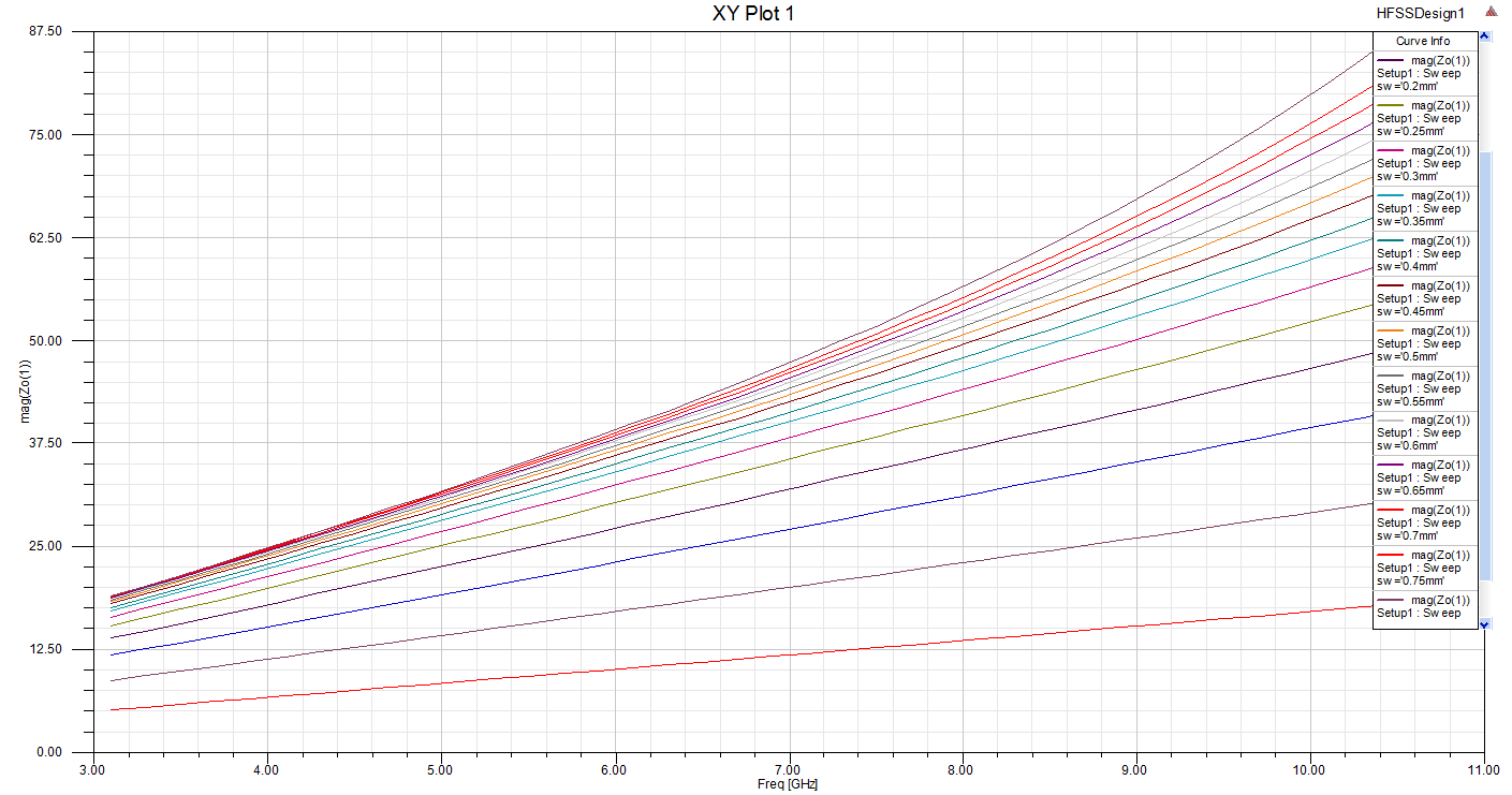
The simulation (ports only, 3.1...10.6 GHz with f_c=6.85GHz) converges and gives out some results which are way smaller than what I expect due to closed form equations in [Janaswamy, Schaubert - 1986].
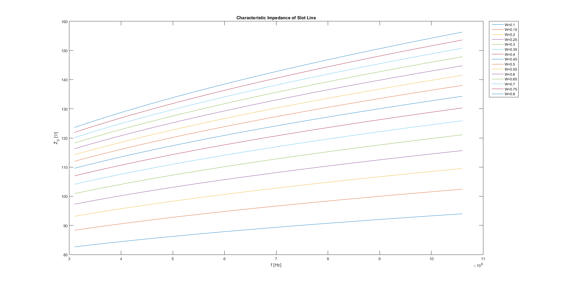
I calculaed the characteristic impedance using eq. 9 for W=0.1...0.8mm (since it is not valid for 0.05mm) in the above paper and plotted the result comparing it to the simulated results:
Does anyone have a hint for me? Is there a problem with the simulation or does the equation just not hold for my case for some reason?
Best regards,
Daniel
Exact values: width is 10*g and hight is 5*h.
Started with ports only but the reported graphs above have been calculated completely (not ports only).
Sorry for reporting imprecisely
as I am having some trouble with my antenna design, I started splitting it up in small problems:
My very first problem is about designing a slot line and determining it's characteristic impedance Z_0.
My simulation is quite easy:
I have defined a slot line on a low dielectric (epsilon_r=3.5) substrate (h=251μm). The slot line width is varied between 0.05mm and 0.8mm.
I put an air box around the structure at lambda/4 distance with radiation boundary (which is actually not needed here - I just put it to be sure not to have problems with any reflections).
At each end of the slot line I put a waveport with integration line defined from one conductor to the other and Z_0 calculated by Z_pv. The port is defined on a rectangle as it has to be (Width = ~ 7g and height > 4h or 4g). I tried PEC port caps as well as having the air box terminated at the ports.
The simulation (ports only, 3.1...10.6 GHz with f_c=6.85GHz) converges and gives out some results which are way smaller than what I expect due to closed form equations in [Janaswamy, Schaubert - 1986].
I calculaed the characteristic impedance using eq. 9 for W=0.1...0.8mm (since it is not valid for 0.05mm) in the above paper and plotted the result comparing it to the simulated results:
Does anyone have a hint for me? Is there a problem with the simulation or does the equation just not hold for my case for some reason?
Best regards,
Daniel
Exact values: width is 10*g and hight is 5*h.
Started with ports only but the reported graphs above have been calculated completely (not ports only).
Sorry for reporting imprecisely
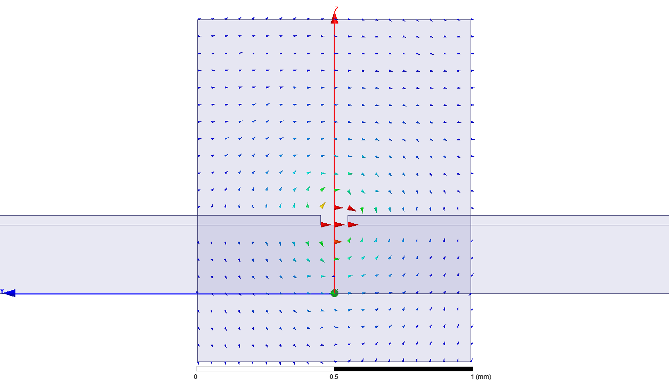
Are the fields correct on the port?
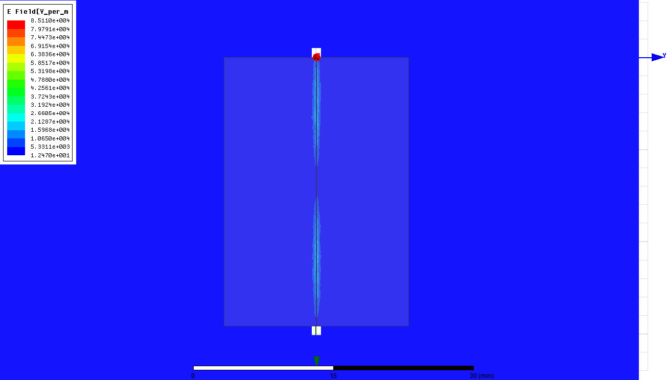
I think they look fine. I attached the Field display as well as the mag(E) at the port.
Furthermore I attached the mag(E) field on the slot line.
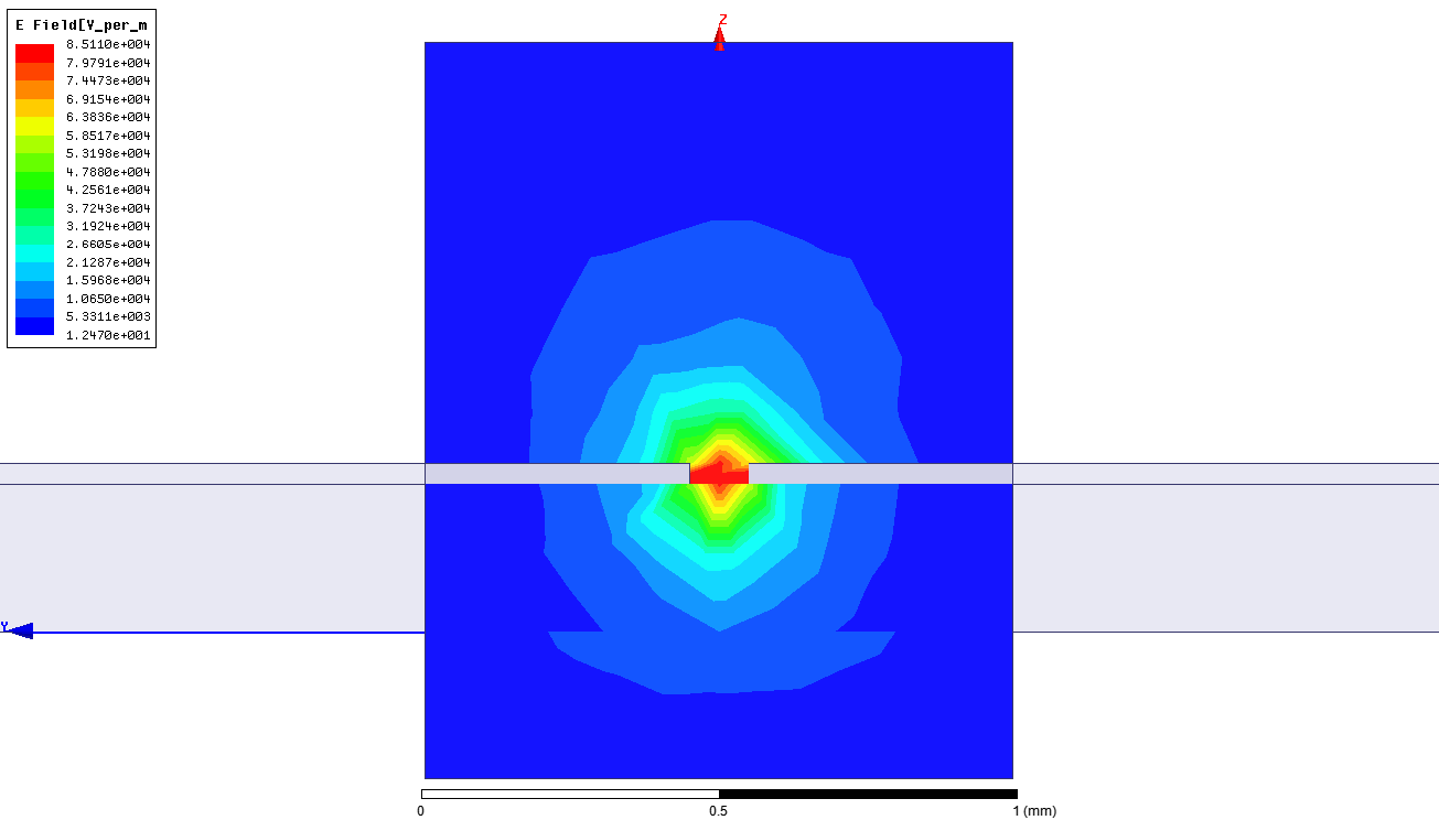
That does look fairly correct. Does the formula you used take into account the thickness of the traces? They look pretty thick with respect to the width of the gap -- this can have a large effect on the solution.