Through-hole via in Agilent Momentum
时间:03-30
整理:3721RD
点击:
I want to insert multi-layer via into and I drew one using this tutorial.
https://abhargava.files.wordpress.co...-using-ads.pdf
The problem is that in the tutorial, they simulate via filled with conductor. What I want is a through hole via with metal thickness of several mil that is open and the two conducting planes do not cover it.
https://abhargava.files.wordpress.co...-using-ads.pdf
The problem is that in the tutorial, they simulate via filled with conductor. What I want is a through hole via with metal thickness of several mil that is open and the two conducting planes do not cover it.
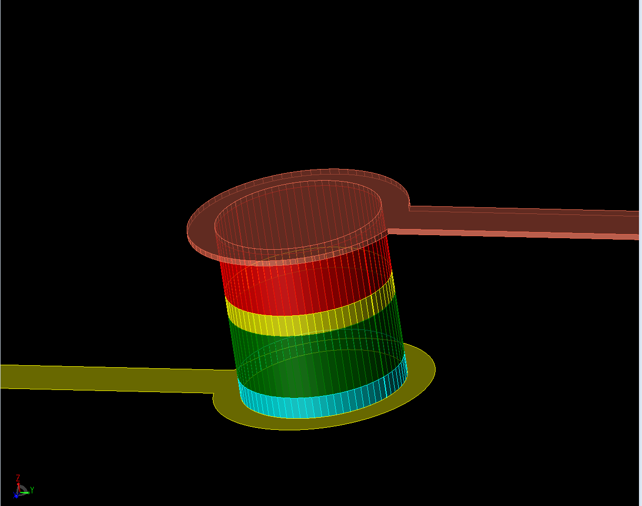
Skin effect will cause current flow on the via surface only, so it makes no difference in results if you model a hollow via or filled. Current flows on the surface only in both cases.
That was the physics part. Now the tool part: Momentum internally meshes the surface of conductors, so that the EM solution uses a "hollow" via anyway. You could draw the via as a donut, but it really makes no difference except for the effective series resistance that Momentum uses for the via side walls.
For the pad, you can draw them as a donut if you wish. To cut out the center, draw a circle with the hole diameter on the metal layer, then use Edit > Merge > Union Minus Intersection.