Creating a new component on ADS
How can i create a new componente in ADS ? I have the SPICE parameters of a schottky diode (SMS 7630-040LF), parasitics package values and the dimensions.
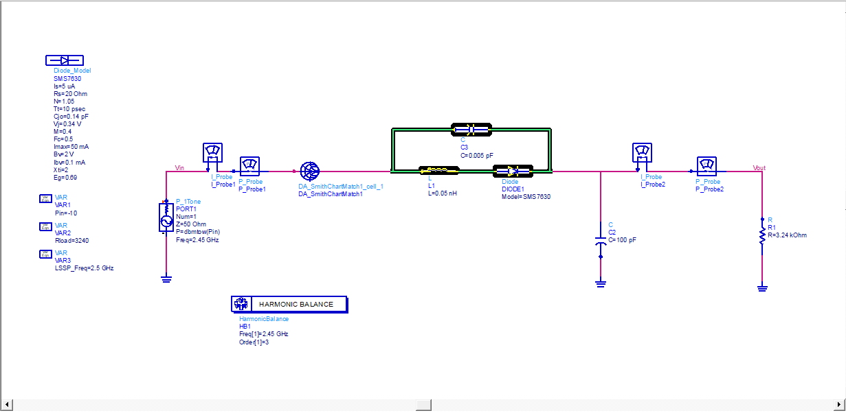
I want to put this parasitcs values(Series inductance,parallel capacitance) and the diode model in to a single component. So how can i do that?
Thank you
Create a new cell in ADS with these views:
schematic with equivalent circuit model and 2 pins (pins for the toolbar, not TERM for ports)
component layout with footprint from datasheet and pins
symbol that you copy from an existing library diode
Then you can use that cell in your designs.
Hi Dr. Volker, i made your suggestion, but i have a little doubt in my footprint design, i'm totally new on it...I made my footprint on ads, following the datasheet dimensions (on the left side)

But i don't understand the right side of the datasheet, all these dimensions, i mean, should i put all these things (PCB pad metalization and PCB solder mask opening) or just that :

Thank you
ADS is essentially not a PCB Design Program so placing Solder Resist Mask or other Stuffs has no sense at all.
Also, parasitic effects will not truly be represented with this Footprint.Layout of ADS is meaningful when the Distributed Components are used suh as Microstrip Lines,Sheet Filter,Lange Coupler etc.
For circuit simulation, you don't need the component layout, only symbol and schematic.
If you want to use the circuit layout, for PCB production or for EM simulation, you must define the component layout.
For EM simulation, I would draw the pad dimensions (that has an effect if you use Momentum EM simulation) and a case outline (to show component placement and distance to the user). Add pins to the pads, for making the connection to the circuit, and that's all you need for EM.
If you want to use ADS for creating the layout files for manufacturing (Gerber), then you also need to define solder mask.
So, if i want take in count parasitc effects what should i do?
All right, understood! I want to fabricate this circuit to test in a spectrum analyser, you recommend me to use another software or not?
ADS should be fine for creating the layout, many people use that.
If your PCB has solder resist layer, you need to define that layer in your SMD footprint.
Regarding layout parasitics, you can do EM simulation of the overall circuit (most accurate, but not so easy to get started, many details to consider), or include the pads as circuit simulation models with the pad size specified. This give the correct shunt parasitics.
To get the right amount of series path length, you would model the pad as a piece of line (to component reference plane) plus some open ended stub. The physical size of the diode itself is already included in your model (the series inductance). What you need really depends what you required level of accuracy is, and how much which parasitics matter at your operating frequency.
Dr. Volker Can you recommend me some videos or material that shows all these considerations you are talking (i mean modelling the pad and stuff)? I can't see all these things yet and i don't want bothering you with all these questions... but i need a accurate model to fabricate, i need to write an article to present at my university...
I wish that material would exist ... unfortunately I don't know tutorials that summarize all this. I am working as an EM simulation expert for almost 20 years now, and had to learn these things over time, to see what effects matter and what isn't relevant. Overall, it's mostly simple physics, and some simplified view often helps to understand what the circuit is sensitive to.
When it comes to connecting EM and components (measured data), it is sometimes guessing what reference plane was used in measurement: at the package body, or measurement includes some lead/pad length, and what pad capacitance is perhaps in the data (or not) that depends on the substrate used for measurement. In your case, by looking at the diode model, I see no shunt elements so the pads are NOT included. My interpretation (educated guess) of the series L is that this models the physical size of the diode itself. So I would place the EM pins for the diode at the center of the pads.
Good luck!
Volker
- Creating a matching network for an HFSS antenna array in Ansoft Designer
- Problem with creating a transformer using CoilSys - ADS 2017
- Problem with Keysight ADS EM simulation
- Re: Confused - transmission line component in Virtuoso and ADS
- ADS:Error while adding bat54 component in ads layout from HFDiode library
- ADS and S11 Equations for L & C