Slew Rate—the op amp speed limit
Slewing behavior of op amps is often misunderstood. It’s a meaty topic so let’s sort it out.
The input circuitry of an op amp circuit generally has a very small voltage between the inputs—ideally zero, right? But a sudden change in the input signal temporarily drives the feedback loop out of balance creating a differential error voltage between the op amp inputs. This causes the output to race off to correct the error. The larger the error, the faster it goes… that is until the differential input voltage is large enough to drive the op amp into slewing.
If the input step is large enough, the accelerator is jammed to the floor. More input will not make the output move faster. Figure 1 shows why in a simple op amp circuit. With a constant input voltage to the closed-loop circuit there is zero voltage between the op amp inputs. The input stage is balanced and the current IS1 splits equally between the two input transistors. With a step function change in Vin, greater than 350mV for this circuit, all the IS1 current is steered to one side of the input transistor pair and that current charges (or discharges) the Miller compensation capacitor, C1. The output slew rate (SR) is the rate at which IS1 charges C1, equal to IS1/C1.
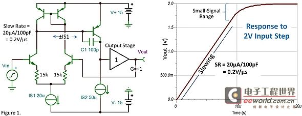
There are variations, of course. Op amps with slew-enhancement add circuitry to detect this overdriven condition and enlist additional current sources to charge C1 faster but they still have a limited slew rate. The positive and negative slew rates may not be perfectly matched. They are close to equal in this simple circuit but this can vary with different op amps. The voltage to slew an input stage (350mV for this design) varies from approximately 100mV to 1V or more, depending on the op amp.
While the output is slewing it can’t respond to incremental changes in the input. The input stage is overdriven and the output rate-of-change is maxed out. But once the output voltage nears its final value the error voltage across the op amp inputs reenters the linear range. Then the rate of change gradually reduces to make a smooth landing at the final value.
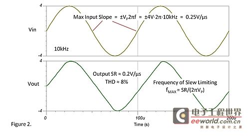
There nothing inherently wrong with slewing an op amp—no damage or fines for speeding. But to avoid gross distortion of sine waves, the signal frequency and/or output amplitude must be limited so that the maximum slope does not exceed the amplifier’s slew rate. Figure 2 shows that the maximum slope of a sine wave is proportional to VP and frequency. With 20% less than the required slew rate, output is distorted into a nearly triangle shape.
Large-signal square waves with very fast edges tilt on the rising and falling edges according to the slew rate of the amplifier. The final portion of a rising or falling edge will have rounding as the amplifier reaches its small-signal range as shown in figure 1.
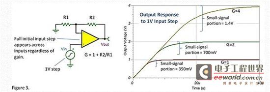
In a non-inverting circuit, a minimum 350mV step is required to make this op amp slew, regardless of gain. Figure 3 shows the slewing behavior for a 1V input step with gains of 1, 2 and 4. The slew rate is the same for each gain. In G=1, the output waveform transitions to small-signal behavior in the final 350mV. In G=2 and G=4 the small-signal portion is proportionally larger because the error signal fed back to the inverting input is attenuated by the feedback network. If connected in a gain greater than 50, this amplifier would be unlikely to slew because a 350mV step would overdrive the output.

Slew rate is usually specified in V/μs, perhaps because early general purpose op amps had slew rates in the range of 1V/μs. Very high speed amplifiers are in the 1000V/μs range, but you would rarely see it written as 1kV/μs or 1V/ns. Likewise, a nanopower op amp might be specified as 0.02V/μs but seldom as 20V/ms or 20mV/μs. There’s just no good reason why for some things; it’s just the way we do it. :-)
I’ve exceeded my word limit yet again! Thanks for hanging in and comments are welcome.
Bruce
运放的压摆动作经常被误解。压摆率是一个内容较多的话题,我们需要将它进行分类讨论。
运放输入级电路的两个输入端之间的电压通常非常小------理想情况下为零,对吗?但是,输入信号突然地改变会短暂打破反馈回路的平衡,在运放的输入端产生一个误差差分电压。这将会导致运放的输出产生变化来校正输入端的误差电压。误差电压越大,输出端电压变化得越快,直到输入端的差分电压足够大从而使得运放产生压摆。
如果输入足够大的信号,意味着加速器已经踩到了底,输出信号不可能变化得更快了。更大的输入并不会使输出变化得更快。图1用一个简单的运放电路解释了这个原因。闭环回路上有一个恒定的电压,使得运放输入端之间的电压为零。输入级的两个输入端之间是平衡的并且电流IS1相同地分配到三极管的两个输入端。对于该电路,当输入信号Vin是大于350mV的阶跃信号时,电流IS1只流向输入差分对管的一个三极管,该电流对米勒补偿电容C1充电或者放电。输出压摆率SR是IS1对C1充电的比例,等于IS1/C1。

当然,有各种各样的运放电路来改善压摆率。有压摆增强电路的运放用来检测这种过载条件并且获得更多额外的电流来给C1快速充电,但是在这种情况下,压摆率还是受限制的。正端和负端的压摆率可能不完全相同。在这种简单的电路中,正端和负端的压摆率是接近相等的,但是在不同的运放中,这可能会随之变化。输入级的压摆信号(本设计是350mV)可以从100mV到1V或者更多,这取决于不同的运放。
但是输出端的压摆不能响应输入信号的改变。输入端过载时,输出端不能随之发生变化。但是一旦输出电压接近其最终值,输入端的误差电压重新出现在线性区,变化率逐步减小,最终得到一个平滑的稳定值。
在运放压摆时,并没有内在的错误------对速度没有减小或提升。但是为了避免正弦信号的严重失真,信号的频率和输出信号的幅度必须有一定的限制以保证输出信号的最大斜率不会超过运放的压摆率。图2中,正弦信号的最大斜率是正比于幅度Vp和频率的。如果压摆率较小(小于所需压摆率的20%),输出信号将会失真,类似于一个三角波。
对运放的压摆率来说,幅度较大的方波信号有非常陡的上升沿和下降沿。最终,一部分上升和下降沿被平滑为运放的小信号,如图1所示。
在同相电路中,不管增益是多少,350mV的输入阶跃信号将会使运放产生压摆。图3显示了输入信号为1V,增益分别为1,2,4时运放的压摆。在不同的增益下,压摆率是相同的。增益为1时,输出波形最终转换为350mV。在增益为2和4时,小信号的比例随之变大,因为反馈到反向输入端的误差信号被反馈网络衰减。如果增益大于50,该运放可能不会压摆因为350mV的输入阶跃信号将会使输出饱和。
压摆率的单位通常是V/us,也许是因为早期的通用运放的压摆率在1V/us左右。高速的运放有1000V/us的压摆率,但是你很少看见它被表达为1kV/us或者1V/ns。而且,低功耗的运放可能写为0.02V/us,而不写为20V/ms或者20mV/us。并没有很好的原因来解释,这只是我们衡量压摆率的一种习惯。