Pushing the precision envelope
The first challenge for system engineers in precision measurements is to choose the best possible performance op amp along with other components surrounding it. This task isn’t trivial, however. In some applications where space is limited, engineers often look for the smallest possible package, but the advantage of a smaller package may not offer the desirable precision.
This article discusses several techniques used by IC manufacturers to overcome the precision challenge and gives the reader a better understanding of the various methods used pre- and post-packaging to provide the best possible performance, even in the smallest packages.
Defining precision analog
How engineers define precision in operational amplifiers (op amps) very much differs and depends greatly on the application. Among the tens of thousands of amplifiers from more than a dozen vendors, engineers often are faced with the challenge of choosing the best possible value. That is, the best performance for the price – given that other components still need to be part of the system.
For instance, a vibration analysis application for oil exploration or seismic study requires amplifiers with very low input offset voltage and drift over time and temperature. This ensures minimal impact on the digitized signal. In other words, a precise op amp with low noise will not severely degrade the high resolution data converter’s performance to provide better accuracy. Conversely, a glucose monitor typically has much less stringent requirements on offset and temperature drift.

Figure 1. A typical block diagram of a portable vibration meter.
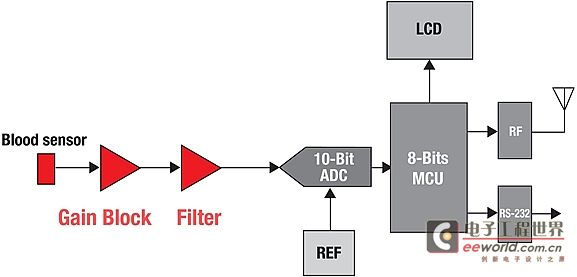
Figure 2. A typical block diagram of a glucose monitor.
Most semiconductor companies tend to agree on the terms of definition for what precision means in op amps. In fact, they tend to group. Op amps are usually grouped under precision, if they have less than 1 mV of initial offset voltage and are below 50 MHz of unity gain bandwidth. However, this level of precision can vary as a function of the process technology, and even in the same device. It is not uncommon to see the same amplifier with two lines of different specifications according to the package choice. This is because smaller packages are more prone to stress from the package molding pushing against the die.
Historically, bipolar input devices held the lead for precision. While some would argue that that they are still the best (and in many ways they are), recent designs in CMOS and JFETs have seen tremendous improvements. An example of JFET input amplifier is the OPA140, which offers 120 uV maximum offset voltage and only 1 uV/°C of offset drift over the extended industrial temperature range.
Achieving precision without chopping
Just like system engineers, IC designers use various techniques at the IC level to achieve a high level of precision. One way IC designers can attain such level of precision is to implement chopper stabilization or auto zeroing independently or in conjunction. Although, these techniques can be very effective there are some drawbacks associated with them which can make these amplifiers undesirable in some applications. To counter this, many manufacturers offer trimming methods at the IC level to provide a much lower offset voltage. This in turn can enhance the drift over temperature. However, not all trimming methods have the same benefits. Some may not be appropriate for certain designs targeting cost-sensitive applications. Usually, a decision is made once the product is defined and the target applications are identified.
To trim or not to trim
One of the oldest trimming techniques is Zener-zapping, which has been done on many precision amplifiers. This technique is generally performed on larger geometries and doesn’t prove to be cost effective on smaller geometry processors like CMOS. Zener-zapping is an on-chip technique. Although very good precision can be attained, it usually requires a larger die area, making it difficult to fit into a small package.
Laser trim is a popular approach in precision devices and offers the advantage of fewer test pads and reduced cost over link trim. It is used widely in difference and instrumentation amplifiers to improve resistor matching and provide the necessary common-mode rejection ratio (CMRR). However, it lacks the capability of post-assembly trimming.
EEPROM is yet another on-chip technique that can be used, but seldom on standalone amplifiers as it often requires additional pins and extra masks.
As the demand for precision keeps increasing, many manufacturers now can provide post assembly trimming. These polysilicon fuse-blowing techniques do not require extra pins or test pads and provide substantial cost savings over prepackage trim methods. This is a true breakthrough in technology as many CMOS amplifiers now can achieve unprecedented levels of DC precision, namely sub-hundred microvolts of initial offset and sub one microvolt of offset drift. The DC parameters can be appreciated in the OPA376, a CMOS input amplifier with 25 μV of guaranteed offset voltage.
Post assembly trimming allows IC designers and layout engineers to overcome the induced mechanical stress in very small packages and, therefore, can offer excellent precision in miniature sizes. In addition to cost savings, the implementation of such techniques on CMOS enables the use of lower voltages. The lower supply offers users longer battery life essential in portable applications, and helps save power in high-density boards, in addition to providing an easy interface with logic devices and microcontrollers.
Table 1 summarizes the various trimming methods and classifies them by pre- and post-assembly, according to technology and manufacturer.
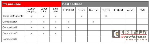
Table 1. Summary of trimming methods.
Choosing precision according to trimming
Choosing an amplifier’s precision according to trim method can be misleading. Post-assembly trimming sometimes is done at a specific trim point. To maintain the lowest offset and temperature drift the design may require additional complex circuitry, which can add substantial real estate to the die area. Look beyond the first page of the datasheet specification table to determine the actual value of the offset and its variation over the common mode, rather than rely on the trim algorithm branding.
Some manufacturers rely on the success of the precision device to launch untrimmed versions,which can target a different set of applications. This can be beneficial to both the IC vendor and the customer alike by reducing the cost with minimal effort.
References
Download a datasheet for the OPA376: www.ti.com/opa376-ca.
For more information on op amps from TI, visit: www.ti.com/opamps-ca.
About the author
Soufiane Bendaoud is a business development manager for TI’s Precision Analog group. Soufiane received here a BSEE degree from San Francisco State University and a MBA from the University of San Francisco.
Pure English
可以翻译一下吗?美女!