高速DDR PCB设计中的时序分析
高速DDR PCB设计中的时序分析
A)DDR System Implementation Guidelines:
Since DDR devices using a 200MHz clock (“DDR400”) are used, the memory architecture provides a theoretical peak bandwidth of:
2 (controllers) * 4 (bytes/controller) * 400 (Mtransfers/sec) = 3.2 Gbytes/sec
Key features of this topology include the following:
1. All data signals (DQ, DQS, DM) can be routed with a maximum trace length of 1500mils or less.
2. All address, command, and clock signals can be routed with a maximum trace length of 2000 mils or less.
3. Series termination – nominal 33 ohms – is recommended for all DRAM signals
4. Differential clock signals should be routed as a differential pair, targeted for a differential impedance of 100 ohms (each clock trace 50 ohms)
5. Designs should use the following PCB track width and clearance rules:
Signal Group Track Width Clearance
DQSx 5 10
CK/CK# Target to 100R
differential impedance 10
All others 5 5
B) 6层板参考层结构为:信号1(顶)、地平面、信号2 信号3 电源平面、信号4(底)。各层间距依次可为8mil 8mil 14mil 8mil 8mil。
假定板材介电常数4.2, 铜厚1oz
芯片之间的走线长度估计在2500-3500mil左右, 匹配采用串联终端的匹配, 芯片数据手册如图.
怎样进行时钟和数据的信号完整性进行分析仿真?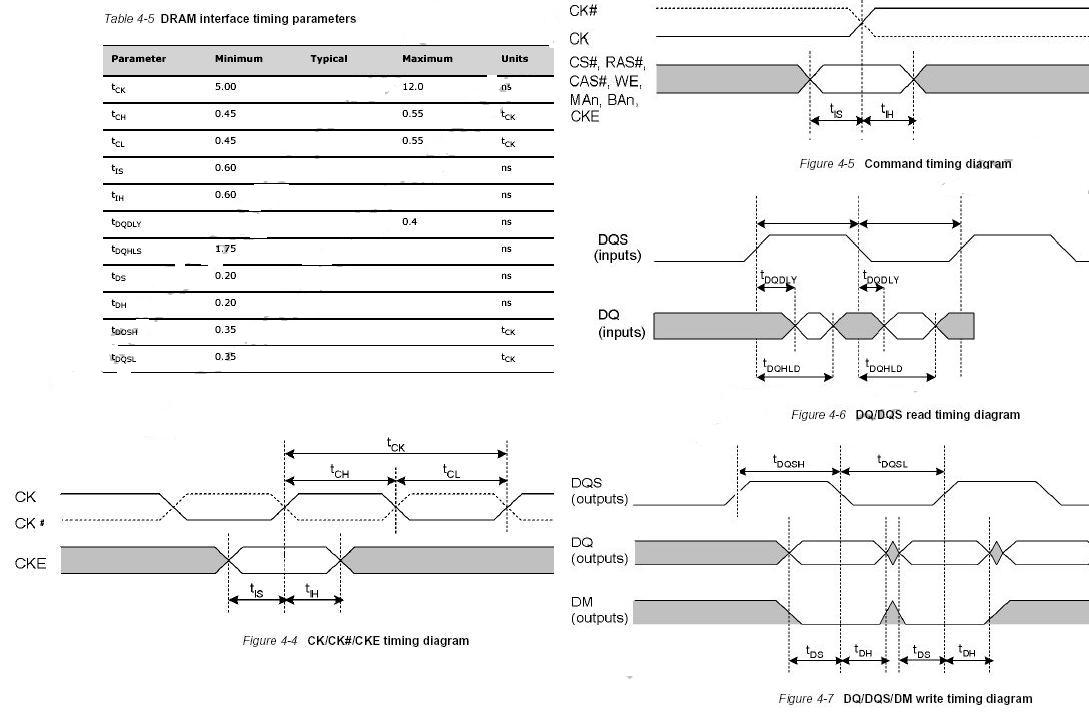
麻烦小编再说的详细一点?
高手.谢谢
请问小编,您上面所说的那段英文资料在哪儿本书里可以找到,急需!谢谢!
你提供的资料只是DDR要满足的时序要求,还要看你的控制器是什么,能提供什么样的时序,控制器需要什么样的时序。控制器和DDR接口要满足四个量,DDR的SETUP TIME, HOLD TIME 和控制器的SETUP TIME, HOLD TIME 。
是啊,请问小编还有更详细的资料吗?谢谢!
4楼的要什么我给你,那些资料多的是。
那个最大长度是怎么得出了的啊?
谢谢!
Good luck!
怎么没有下文了啊