能做50~60层板的厂商
这是今天我在读《Handbook of digital techniques for high-speed design》一书 第12章 high-speed interconnects and cabling 时看到的,这本书是2004年出版的,当时TDA System 还没给Tek 收购,Teradyne 背板连接器部门也还在独立运作。
7年过去啦,能做60层板的厂商又多了一些,大家能讨论一下吗?
森马仕能做8mm的背板吗?
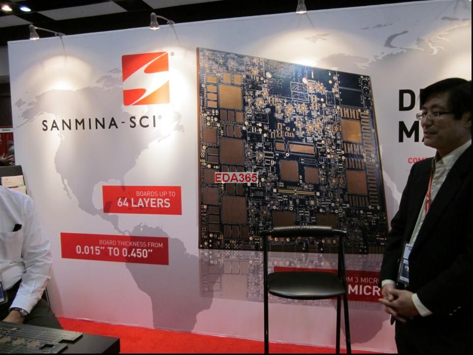
Figure 1 illustrates the channel insertion loss of a 30-in. differential channel with differential vias at each end. Using short vias with no stubs (green, top trace), the response rolls off smoothly to −13 dB at 5 GHz. Thick backplane vias with long stubs (red) create unwanted resonances in the channel insertion loss, whereas vias with short or no stubs do not. If these resonances occur near the Nyquist frequency of the bit rate, they will devastate the eye opening at the receiver.
Stub resonances occur when a portion of the signal traversing the active region of a via diverts down into the stub section, reflects off the open-circuited end, and returns later to recombine with the main signal. At a high frequency-the quarter-wave resonant frequency-the round-trip delay from the active region of the via to the end of the stub and back equals a half-cycle. If this scenario occurs, the main wave and the reflected wave appear 180° out of phase, producing destructive signal cancellation. The longer the stub, the lower the resonant frequency is.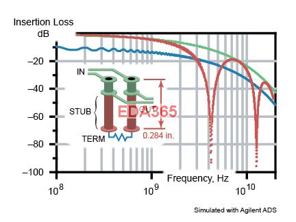
Figure 1—In this simulation, using Agilent's ADS, the channel insertion loss represents two differential vias with 30 in. of PCB etch. This loss deteriorates significantly when you use long vai stubs (red), as opposed to short, back-drilled vias (green).
You can shorten your backplane's via stubs by back-drilling the vias as close as possible to the active internal-signal layer. This complex and costly process requires that you specify the necessary back-drilling depth for each via using special design features in your artwork. Occasionally, glitches in the back-drilling process leave some vias with longer-than-expected stubs. It is only after the board has been fully assembled and tested in the system that such a problem can show up in the form of a higher biterror rate.
Some vias can never be adequately back-drilled. For example, you must maintain a minimum via barrel length to ensure mechanical stability and good electrical contact to a press-fit connector pin. If that pin connects to a signal layer shallower than the minimum required press-fit via length, the protruding portion of the via creates a longer-than-optimum stub.
Because using via stubs seems unavoidable, what is the alternative? Nicholas Biunno, PhD, principal scientist at Sanmina-SCI Corp, suggests terminating them. Sanmina has developed the new MTS (matched-terminated-stub) via technology, which embeds tiny metal thin-film or polymer thick-film resistors within a PCB (printed-circuit-board) stackup during fabrication. The technology can terminate a differential-via stub, thus preventing reflections. With one resistive layer at the bottom of your PCB stackup, you can terminate all the high-speed via stubs in your design. Experiment with your favorite field solver to find the right value of resistance. As Figure 1 shows (blue trace), you can eliminate the resonant notches at the cost of additional flat-loss attenuation.
This stub-termination technology looks like a promising alternative to back-drilling, resolving many of its limitations. Combining it with silicon that can accommodate the additional signal loading may extend the life of traditional copper interconnections for the next generation of Ethernet standards beyond 10 Gbps.
看见TERADYNE了
几年前我们能做到四十多层,不过现在这种高层数的需求貌似很少,只有巨型机上用。小编你们那能到多少现在。
这是我们公司
60层,不知道用在什么地方……
参与过一个56层的背板,11mm厚,不知道在哪里做的。
Mulltek是伟创力国际集团属下的一间世界领先的跨国性专业印刷电路板制造商,制造包括BGA基板和六十八层背板在内的各种印刷电路板产品。
我以前公司的PCB供应商就是SANMINA
只见过二十层
谁能展示一下这种厚度超1cm,长度超1m 背板的通道阻抗、ILD控制水平就好啦,大背板走线之间的一致性绝对是挑战。
我司设计过50多层的背板,苦于厂商难找。
那看来你们公司也挺牛的,做这么多层数,接近1cm的背板。
你们什么公司啊?能有这么大的板子需求?哪最后在哪加工的啊?