关于电容两个焊盘的处理疑问
时间:10-02
整理:3721RD
点击:
最新拿到一家IC厂家的推荐设计文件
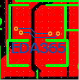
发现里面的大封装电容的两个焊盘全部贴的很近,1206封装的电容,焊盘间距大概只有10mil左右。
The +V and GND traces between the capacitors should be as close to each other as possible.so that the gap between the two nodes is minimized.
这样处理的意义何在?
减小ESR吗?
发现里面的大封装电容的两个焊盘全部贴的很近,1206封装的电容,焊盘间距大概只有10mil左右。
The +V and GND traces between the capacitors should be as close to each other as possible.so that the gap between the two nodes is minimized.
这样处理的意义何在?
减小ESR吗?