CAT6500自动电源选择开关详细介绍
CAT6500 is an automatic power switch designed to select between two power sources and direct that power to a load for battery charging or system power.
CAT6500’s power inputs withstand voltages of up to 18 V and protect the downstream load from voltages exceeding 7V. In the event of a polarity reversal at either input CAT6500’s internal power switches will shut off to prevent discharge of the system’s internal power source.
功能框图:
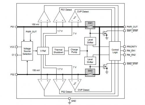
CAT6500功能框图
管脚定义:
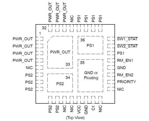
CAT6500管脚定义
引脚功能描述:
| Pin No. | Pin Name | Description |
|
| 1, 2, 3, 4 | PWR_OUT | Power Output. Must be tied to PWR_OUT on opposite side of chip. Use all 3 pins each side. |
|
| 5 | NIC | No Internal Connection. A signal or voltage applied to this pin will have no effect on device operation. |
|
| 6, 7, 8, 9, 10 | PS2 | Power Source #2. External power input |
|
| 11, 12 | NIC | No Internal Connection. A signal or voltage applied to this pin will have no effect on device operation. |
|
| 13 | VCC | Power input from battery. |
|
| 14 | GND | Ground. Reference point for all voltages. |
|
| 15 | C1 | Filter capacitor for CAT6500’s internal power bus |
|
| 16 | NIC | No Internal Connection. A signal or voltage applied to this pin will have no effect on device operation. |
|
| 17 | NIC | No Internal Connection. A signal or voltage applied to this pin will have no effect on device operation. |
|
| 18 | PRIORITY | Priority selects preferred power source when both PS1 and PS2 are powered. |
|
| 19 | RM_EN2 | Reverse Mode Enable 2. Overrides PRIORITY and turns SW2 ON. |
|
| 20 | GND | Ground. Reference point for all voltages. |
|
| 21 | RM_EN1 | Reverse Mode Enable 1. Overrides PRIORITY and turns SW1 ON. |
|
| 22 | PS1 | Power Source #1. External power input. |
|
| 23 |
SW2_STAT | Power Source 2 Status. An open drain LOW true logic level output indicating that the switch SW2 is |
|
|
| |||
| 24 |
SW1_STAT | Power Source 1 Status. An open drain LOW true logic level output indicating that the switch SW1 is |
|
|
| |||
| 25, 26, 27, 28 | PS1 | Power Source #1. External power input. |
|
| 29 | NIC | No Internal Connection. A signal or voltage applied to this pin will have no effect on device operation. |
|
| 30, 31, 32 | PWR_OUT | Power Output. Must be tied to PWR_OUT on opposite side of chip. Use all 3 pins each side. |
|
| 33 | PWR_OUT | Electrically active thermal pad. Does not need to be connected to other PWR_OUTs. Can be lef |
CAT6500 ON SEMICONDUCTOR 相关文章:
- CAT6500自动电源选择开关简述(07-27)
- CAT6500自动电源选择开关应用指南(07-27)
- CAT6500自动电源选择开关应用手册(独家)(08-12)
- DPA-Switch为应对PoE受电设备设计挑战提供有效解决方案(11-06)
- 在射击探测器中增加口径确定功能的简单电路(11-13)
- 高效率PFC电路二极管选择方案(01-24)