STM32_GPIO配置及库函数讲解——独立按键
d as system clock source */
while(RCC_GetSYSCLKSource()!=0x08){}
}
/* Enable GPIOC and GPIOB clock */
RCC_APB2PeriphClockCmd(RCC_APB2Periph_GPIOB,ENABLE);
RCC_APB2PeriphClockCmd(RCC_APB2Periph_GPIOC,ENABLE);
}
/*******************************************************************************
* Function Name : NVIC_Configuration
* Description : Configures Vector Table base location.
* Input : None
* Return : None
*******************************************************************************/
voidNVIC_Configuration(void)
{
#ifdefVECT_TAB_RAM
/* Set the Vector Table base location at 0x20 */
NVIC_SetVectorTable(NVIC_VectTab_RAM,0x0);
#else/* VECT_TAB_FLASH */
/* Set the Vector Table base location at 0x08 */
NVIC_SetVectorTable(NVIC_VectTab_FLASH,0x0);
#endif
}
/*******************************************************************************
* Function Name : GPIO_Configuration
* Description : Configures the different GPIO ports.
* Input : None
* Return : None
*******************************************************************************/
voidGPIO_Configuration(void)
{
GPIO_InitTypeDef GPIO_InitStructure;
/* Configure PC.06, PC.07, PC.08 and PC.09 as Output push-pull */
GPIO_InitStructure.GPIO_Pin=GPIO_Pin_6GPIO_Pin_7GPIO_Pin_8GPIO_Pin_9;
GPIO_InitStructure.GPIO_Speed=GPIO_Speed_50MHz;
GPIO_InitStructure.GPIO_Mode=GPIO_Mode_Out_PP;
GPIO_Init(GPIOC,&GPIO_InitStructure);
/* Configure PB.09 as Input pull-up */
GPIO_InitStructure.GPIO_Pin=GPIO_Pin_9;
GPIO_InitStructure.GPIO_Mode=GPIO_Mode_IPU;//上拉输入
GPIO_Init(GPIOB,&GPIO_InitStructure);
}
/*******************************************************************************
* Function Name : Delay
* Description : Inserts a delay time.
* Input : nCount: specifies the delay time length.
* Return : None
*******************************************************************************/
voidDelay(vu32 nCount)
{
for(;nCount!=0;nCount--);
}
#ifdefDEBUG
/*******************************************************************************
* Function Name : assert_failed
* Description : Reports the name of the source file and the source line number
* where the assert_param error has occurred.
* Input : - file: pointer to the source file name
* - line: assert_param error line source number
* Return : None
*******************************************************************************/
voidassert_failed(u8*file,u32 line)
{
/* User can add his own implementation to report the file name and line number,
ex: printf("Wrong parameters value: file %s on line %d\r\n", file, line) */
/* Infinite loop */
while(1)
{
}
}
#endif
还有个问题:PB9的初始状态是什么?或者说GPIO_Configuration函数后PB9管脚上是高电平还是低电平?
这要看GPIO_InitStructure结构体的GPIO_Mode成员变量初始化为什么,如果为上拉,则PB9管脚为高电平;如果为下拉,则PB9管脚为低电平。
GPIO管脚内部电路设计如图:
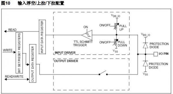
当GPIO初始化为输入上拉模式,由上图可知:该端口向外输出高电平,即:ODR对应位为1
当GPIO初始化为输入下拉模式,由上图可知:该端口向外输出低电平,即:ODR对应位为0
如何调试:在下面两处处设个断点。
1. GPIO初始化函数GPIO_Configuration中
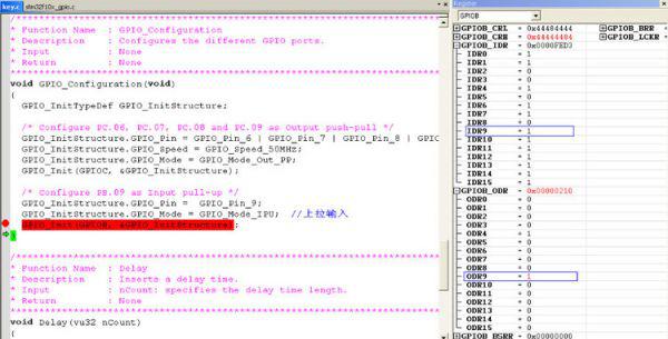
可以看到:当GPIO设置成输入上拉模式时,等待GPIO初始化完毕,该管脚ODR9为1
2. 在main函数中,设置一个断点。
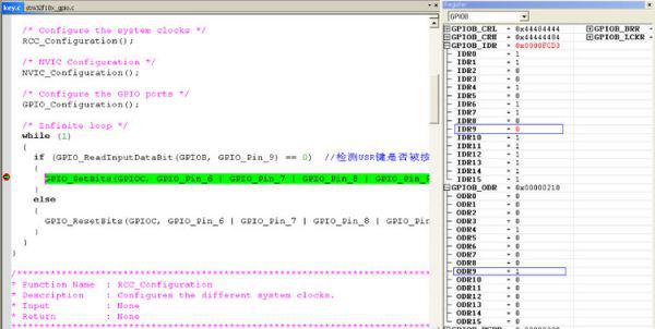
全速执行(F5),按住UserButton不放,可以看到GPIOB_IDR的IDR9=0。当放开按键时,再单步调试(F10),
GPIOB_IDR的IDR9=1。
总结:1. GPIO配置成输入模式时,最好配置成浮空输入(ODR对应位为0)。上拉、下拉只是该管脚初始化完对外表现的电平状态。
2. GPIO配置成输入模式,只关心GPIO_IDR寄存器。检测该管脚外部输入的是高电平还是低电平。
3. GPIO配置成输出模式,只关心GPIO_ODR寄存器。通过该管脚向外部输出高电平还是低电平。
STM32GPIO配置库函数独立按 相关文章:
- Windows CE 进程、线程和内存管理(11-09)
- RedHatLinux新手入门教程(5)(11-12)
- uClinux介绍(11-09)
- openwebmailV1.60安装教学(11-12)
- Linux嵌入式系统开发平台选型探讨(11-09)
- Windows CE 进程、线程和内存管理(二)(11-09)