STM32_GPIO配置及库函数讲解——独立按键
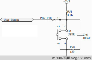
LED硬件连接如下图所示:高电平点亮LED。

要想将PB9管脚配置成输入模式,程序所需如下步骤:(必须的)
第一步:配置系统时钟。见STM32F103xRCC寄存器配置
除此之外,还需将GPIO外设时钟打开。
/* Enable GPIOC and GPIOB clock */
RCC_APB2PeriphClockCmd(RCC_APB2Periph_GPIOB,ENABLE);
RCC_APB2PeriphClockCmd(RCC_APB2Periph_GPIOC,ENABLE);
第二步:配置中断向量表。决定将程序下载到RAM中还是FLASH中。以后讲。
voidNVIC_Configuration(void)
{
#ifdefVECT_TAB_RAM
/* Set the Vector Table base location at 0x20 */
NVIC_SetVectorTable(NVIC_VectTab_RAM,0x0);
#else/* VECT_TAB_FLASH */
/* Set the Vector Table base location at 0x08 */
NVIC_SetVectorTable(NVIC_VectTab_FLASH,0x0);
#endif
}
第三步:配置GPIO的模式。输入模式还是输出模式。STM32_GPIO配置及库函数讲解——LED跑马灯已讲过。
void GPIO_Configuration(void){GPIO_InitTypeDef GPIO_InitStructure;/* Configure PC.06, PC.07, PC.08 and PC.09 as Output push-pull */GPIO_InitStructure.GPIO_Pin = GPIO_Pin_6 GPIO_Pin_7 GPIO_Pin_8 GPIO_Pin_9;GPIO_InitStructure.GPIO_Speed = GPIO_Speed_50MHz;GPIO_InitStructure.GPIO_Mode = GPIO_Mode_Out_PP; GPIO_Init(GPIOC, &GPIO_InitStructure);/* Configure PB.09 as Input pull-up */GPIO_InitStructure.GPIO_Pin = GPIO_Pin_9;GPIO_InitStructure.GPIO_Mode = GPIO_Mode_IPU; //上拉输入GPIO_Init(GPIOB, &GPIO_InitStructure);}第四步:读该管脚上的电平状态。需要介绍一个库函数。
vGPIO_ReadInputDataBit从指定Port指定Pin,读该管脚上的电平状态:
u8 GPIO_ReadInputDataBit(GPIO_TypeDef*GPIOx,u16 GPIO_Pin)
{
u8 bitstatus=0x00;
/* Check the parameters */
assert_param(IS_GPIO_ALL_PERIPH(GPIOx));
assert_param(IS_GET_GPIO_PIN(GPIO_Pin));
if((GPIOx->IDR&GPIO_Pin)!=(u32)Bit_RESET)
{
bitstatus=(u8)Bit_SET;
}
else
{
bitstatus=(u8)Bit_RESET;
}
returnbitstatus;
}
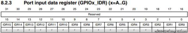
涉及到GPIO_IDR寄存器,如下所示

经过上面4步,就可以检测PB9管脚的电平状态。
按键按下,PB9管脚应该是低电平,怎么才能验证,最简单的方法是:当按键被按下,点亮所有LED。
下面给出完整程序:
/* Includes */
#include"stm32f10x_lib.h"
/* Private function prototypes --*/
voidRCC_Configuration(void);
voidNVIC_Configuration(void);
voidGPIO_Configuration(void);
voidDelay(vu32 nCount);
/*******************************************************************************
* Function Name : main
* Description : Main program.
* Input : None
* Return : None
*******************************************************************************/
intmain(void)
{
#ifdefDEBUG
debug();
#endif
/* Configure the system clocks */
RCC_Configuration();
/* NVIC Configuration */
NVIC_Configuration();
/* Configure the GPIO ports */
GPIO_Configuration();
/* Infinite loop */
while(1)
{
if(GPIO_ReadInputDataBit(GPIOB,GPIO_Pin_9)==0)//检测USR键是否被按下,若按下,则点亮全部LED
{
GPIO_SetBits(GPIOC,GPIO_Pin_6GPIO_Pin_7GPIO_Pin_8GPIO_Pin_9);
}
else
{
GPIO_ResetBits(GPIOC,GPIO_Pin_6GPIO_Pin_7GPIO_Pin_8GPIO_Pin_9);
}
}
}
/*******************************************************************************
* Function Name : RCC_Configuration
* Description : Configures the different system clocks.
* Input : None
* Return : None
*******************************************************************************/
voidRCC_Configuration(void)
{
ErrorStatusHSEStartUpStatus;
/* RCC system reset(for debug purpose) */
RCC_DeInit();
/* Enable HSE */
RCC_HSEConfig(RCC_HSE_ON);
/* Wait till HSE is ready */
HSEStartUpStatus=RCC_WaitForHSEStartUp();
if(HSEStartUpStatus==SUCCESS)
{
/* Enable Prefetch Buffer */
FLASH_PrefetchBufferCmd(FLASH_PrefetchBuffer_Enable);
/* Flash 2 wait state */
FLASH_SetLatency(FLASH_Latency_2);
/* HCLK = SYSCLK */
RCC_HCLKConfig(RCC_SYSCLK_Div1);
/* PCLK2 = HCLK */
RCC_PCLK2Config(RCC_HCLK_Div1);
/* PCLK1 = HCLK/2 */
RCC_PCLK1Config(RCC_HCLK_Div2);
/* PLLCLK = 8MHz * 9 = 72 MHz */
RCC_PLLConfig(RCC_PLLSource_HSE_Div1,RCC_PLLMul_9);
/* Enable PLL */
RCC_PLLCmd(ENABLE);
/* Wait till PLL is ready */
while(RCC_GetFlagStatus(RCC_FLAG_PLLRDY)==RESET){}
/* Select PLL as system clock source */
RCC_SYSCLKConfig(RCC_SYSCLKSource_PLLCLK);
/* Wait till PLL is use
STM32GPIO配置库函数独立按 相关文章:
- Windows CE 进程、线程和内存管理(11-09)
- RedHatLinux新手入门教程(5)(11-12)
- uClinux介绍(11-09)
- openwebmailV1.60安装教学(11-12)
- Linux嵌入式系统开发平台选型探讨(11-09)
- Windows CE 进程、线程和内存管理(二)(11-09)