关于ARM9协处理器CP15及MCR和MRC指令
erations as cache cleaning and lockdown.
这个只读寄存器包含了高速缓存的大小和类型。
The cache type register is accessed by reading CP15 register 0 with the opcode_2 field set to 1.for example:
MRC
The format of cache type register (寄存器的数据格式如下)
Register bits | Function | Value |
[31:29] | Reserved | 000 |
[28:25] | Cache type (缓存类型) | 0110 |
[24] | Harvard/Unified | 1(defines Harvard cache) |
[23:21] | Reserved | 000 |
[20:18] | Data Cache size(数据缓存大小) | 101(defines 16KB) |
[17:15] | Data Cache associativity | 110(defines 64 way) |
[14] | Reserved | 0 |
[13:12] | Data Cache words per line | 10(defines 8 words per line) |
[11:9] | Reserved | 000 |
[ 8:6] | Instruction Cache size(指令缓存大小) | 101(defines 16KB) |
[5:3] | Instruction Cache Associativity | 110(defines 64 way) |
[2] | Reserved | 0 |
[1:0] | Instruction Cache per line | 10(defines 8 words per line) |
寄存器1:Control register
对该寄存器读写指令如下:
MRC
MCR
该寄存器功能如下表
Registe bits | Name | Function | Value |
31 | iA bit | Asynchronous clock select | |
30 | nF bit | notFastBus select | |
29:15 | Read = Unpredictable Write = should be zero | ||
14 | RR bit | Round robin replacement | 0 = Random replacement 1 = Round robin replacement |
13 | V bit | Base location of exception register(异常寄存器基地址) | 0 = Low address = 0x0000 0000 1 = High address = 0xFFFF 0000 |
12 | I bit | Instruction cache enable | 0 = Instruction cache disable 1 = Instruction cache enable |
11:10 | Reserved | Read = 00 Write = 00 | |
9 | R | ROM protection | |
8 | S | System protection | |
7 | B | Big-endian/little-endian | 0 = Little-endian operation 1 = Big-endian operation |
6:3 | Read = 1111 Write = 1111 | ||
2 | C bit | Data cache enable | 0 = data cache disable 1 = data cache enable |
1 | A bit | Alignment fault enable | Data address alignment fault checking (地址对齐检查) 0 = 1 = |
0 | M bit | MMU enable | 0 = MMU disable 1 = MMU enable |
Clocking mode(时钟模式) | iA | |
Fastbus mode (快速总线模式) | ||
Reserved | ||
Synchronous (同步模式) | ||
Asynchronous (异步模式) |
寄存器2:Translation Table Base(TTB) Register
Register bits | Function |
31:14 | Pointer to first level translation table base . |
13:0 | Reserved Read = Unpredictable Write = Should be zero |
访问C2寄存器指令如下:
MRC
MCR
该寄存器存放第一级转换表基地址。写入时,位[13:0]必须为0,读出时,位[13:0]的值不可预知。
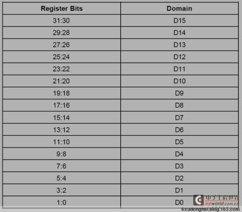
寄存器3:Domain Access Control Register
寄存器3是可读写的域访问控制寄存器,分为16组,每组占用2个位
访问该寄存器的指令如下:
MRC
MCR
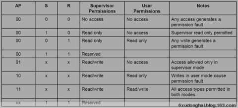
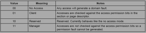
Interpreting Access Control Bits in Domain Access Control Register
寄存器4:保留
对该寄存器的读写会产生不可预料的结果。
寄存器5:Fault Status Register
寄存器6:Fault Address Register
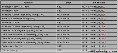
寄存器7:Cache Operations
该寄存器是只写寄存器,用于管理指令缓存和数据缓存。
对该寄存器的写操作所实现的功能,是通过MCR指令中的opcode_2和CRm两者的组合来选择的,具体组合如下。
寄存器8:TLB Operations
Register 8 is a write-only register used to manage the translation lookaside buffer(TLBs),the instruction TLB and the data TLB.
Five TLB operations are defined and the function to be performed is selected by the opcode_2 and CRm fields in the MCR instruction used to write CP15 register 8.Writing other opcode_2 or CRm values id unpredictable. Reading from CP15 register 8 is unpredictable.
ARM9协处理器CP15MRC指 相关文章:
- Windows CE 进程、线程和内存管理(11-09)
- RedHatLinux新手入门教程(5)(11-12)
- uClinux介绍(11-09)
- openwebmailV1.60安装教学(11-12)
- Linux嵌入式系统开发平台选型探讨(11-09)
- Windows CE 进程、线程和内存管理(二)(11-09)