Programmable-Gain Amplifier, Using the MAX532 DAC
Abstract: This application note discusses how to use the MAX532 to build a programmable gain amplifier (PGA) that's suitable for AC gain control. No external components are necessary. Equations are provided to easily calculate the output values.
-- ======================================================================= -->-- CONTENT: DB HTML -->-- ======================================================================= -->The MAX532 is a dual, 12-bit, voltage-output DAC. Access to the output amplifier's input terminals allows it to be easily configured as a programmable-gain amplifier (PGA) suitable for AC gain control.
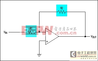
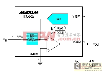
The circuit configuration is that of an inverting amplifier, with R2 replaced by the effective resistance of the DAC ladder (Figure 1) and R1 replaced by internal feedback resistor RFB (Figure 2). In this circuit, an AC signal is applied to the feedback resistor input and the output signal is tied to the DAC reference input. The maximum signal at VOUT is limited by the amplifier's headroom from the supply rails (±12V to ±15V), which must be a minimum of 2.5V from either rail.
Figure 1. Fixed-gain inverting amplifier. 
Figure 2. Programmable-gain amplifier.
The DAC functions as a programmable resistor in the feedback of the amplifier such that :
where R(DAC) is the resistance of the DAC ladder and RFB is the value of the feedback resistor, which is R/2.
R(DAC) = R/2×[4096/(DAC CODE)], with the DAC CODE given as a decimal value. As the code decreases, the effective DAC resistance increases, and so the gain increases. The transfer function for the circuit is thus:
The code can be programmed between 1 and full scale (212-1). Zero code is not allowed, as it results in the DAC's appearing as an open circuit in the feedback loop.
模拟电路 模拟芯片 德州仪器 放大器 ADI 模拟电子 相关文章:
- 12位串行A/D转换器MAX187的应用(10-06)
- AGC中频放大器设计(下)(10-07)
- 低功耗、3V工作电压、精度0.05% 的A/D变换器(10-09)
- PIC16C5X单片机睡眠状态的键唤醒方法(11-16)
- 用简化方法对高可用性系统中的电源进行数字化管理(10-02)
- 利用GM6801实现智能快速充电器设计(11-20)
