How to Reduce Reference Noise
时间:04-11
来源:互联网
点击:
The low-frequency 1/f noise (LF noise) generated by a voltage reference at frequencies below 10Hz is very hard to reduce. One design approach reduces LF noise by implementing a lowpass RC filter, but that requires high-valued capacitors and resistors. High-value capacitors have lower value leakage resistance, which causes voltage error and long-term instability due to an uncontrolled voltage divider with the high-value series resistors. High-value series resistors cause error by undesired voltage drops due to leakage currents and by generating their own thermal noise.
Stacking multiple references will reduce LF noise. By using multiple voltage sources, each composed of a DC source and a noise source, the DC voltages increase linearly and the noise sources (if not correlated) sum geometrically in an RMS fashion. Adding four references, for example, each consisting of a VREF generator and a VNOISE generator, produces the following outputs:

The original ratio of noise voltage to DC reference voltage is divided in half.
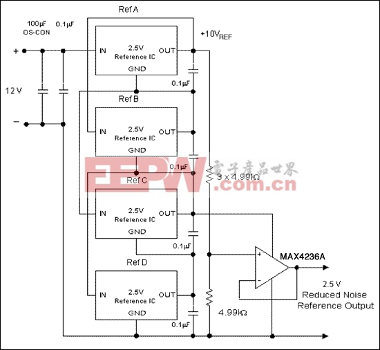
Figure 1 shows how to stack multiple references to generate a single, less noisy reference voltage. The resistors are parts of a high-stability metal-film network, and the op amp is selected for low noise, very low input-offset voltage, and low offset tempco.

Figure 1. Four 2.5V references are stacked to produce 10V. The output is then divided back to 2.5V, which reduces the noise voltage by half.
Two types of 2.5V voltage references can be used in the design. Table 1 and Table 2 show the noise voltages that result from use of either the MAX6037 or the MAX6143 reference. Each table shows the 0.1Hz-to-10Hz noise voltage for the four references individually, and for them in combination. (The dispersion in the ratios of RMS to peak-to-peak (P-P) values is due to some subjectivity in the method used to measure those P-P values.)
Table 1. Noise Voltage Measurements of the Circuit in Figure 1 Using the MAX6037 2.5V Voltage Reference
Table 2. Noise Voltage Measurements of Figure 1 Circuit Using MAX6143 2.5V Voltage References
As an additional benefit of this reference-stack arrangement, the portion of long-term drift due to noise will also be reduced.
A similar version of this article appeared as a Design Idea in the February 3, 2005 issue of EDN magazine.
Stacking multiple references will reduce LF noise. By using multiple voltage sources, each composed of a DC source and a noise source, the DC voltages increase linearly and the noise sources (if not correlated) sum geometrically in an RMS fashion. Adding four references, for example, each consisting of a VREF generator and a VNOISE generator, produces the following outputs:

The original ratio of noise voltage to DC reference voltage is divided in half.
Figure 1 shows how to stack multiple references to generate a single, less noisy reference voltage. The resistors are parts of a high-stability metal-film network, and the op amp is selected for low noise, very low input-offset voltage, and low offset tempco.

Figure 1. Four 2.5V references are stacked to produce 10V. The output is then divided back to 2.5V, which reduces the noise voltage by half.
Two types of 2.5V voltage references can be used in the design. Table 1 and Table 2 show the noise voltages that result from use of either the MAX6037 or the MAX6143 reference. Each table shows the 0.1Hz-to-10Hz noise voltage for the four references individually, and for them in combination. (The dispersion in the ratios of RMS to peak-to-peak (P-P) values is due to some subjectivity in the method used to measure those P-P values.)
Table 1. Noise Voltage Measurements of the Circuit in Figure 1 Using the MAX6037 2.5V Voltage Reference
| Measurement Points | Noise (μVRMS) | Noise(μVP-P) |
| Reduced noise output(op amp, output to V-) | 1.0 | 10 |
| Across Reference A(OUTA to GNDA) | 1.9 | 20 |
| Across Reference B(OUTB to GNDB) | 1.6 | 19 |
| Across Reference C(OUTC to GNDC) | 1.7 | 20 |
| Across Reference D(OUTD to GNDD) | 2.7 | 30 |
Table 2. Noise Voltage Measurements of Figure 1 Circuit Using MAX6143 2.5V Voltage References
| Measurement Points | Noise (μVRMS) | Noise(μVP-P) |
| Reduced noise output(op amp, output to V-) | 0.27 | 2.2 |
| Across Reference A(OUTA to GNDA) | 0.52 | 4.7 |
| Across Reference B(OUTB to GNDB) | 0.60 | 4.8 |
| Across Reference C(OUTC to GNDC) | 0.50 | 4.3 |
| Across Reference D(OUTD to GNDD) | 0.55 | 4.7 |
As an additional benefit of this reference-stack arrangement, the portion of long-term drift due to noise will also be reduced.
A similar version of this article appeared as a Design Idea in the February 3, 2005 issue of EDN magazine.
模拟电路 模拟芯片 德州仪器 放大器 ADI 模拟电子 相关文章:
- 12位串行A/D转换器MAX187的应用(10-06)
- AGC中频放大器设计(下)(10-07)
- 低功耗、3V工作电压、精度0.05% 的A/D变换器(10-09)
- PIC16C5X单片机睡眠状态的键唤醒方法(11-16)
- 用简化方法对高可用性系统中的电源进行数字化管理(10-02)
- 利用GM6801实现智能快速充电器设计(11-20)
