接口数控端口和电阻激光驱动器-Interfacing Dig
时间:04-13
来源:互联网
点击:
This application brief describes the two topologies used to bias optical laser drivers (open loop and closed loop) and demonstrates examples using the DS1847 digital potentiometer and the MAX3273 laser driver. A laser module designer can use a fixed resistor, mechanical pot, digital pot, or a digital-to-analog converter (DAC) to control the laser driver's modulation and bias currents. The advantages of a programmable method (POT or DAC) are that the manufacturing process can be automated and digital control can be applied (e.g., to compensate for temperature). Using POTs can be a more simple approach than a DAC. There can be a slight cost advantage to using a POT, but this is usually not significant relative to other pieces of the design. Using a DAC can offer advantages, including improved linearity (translating to ease of software implementation and ability to hit the required accuracy), increased board density, a wider range of resolutions, a better optimization range, ease of use with a negative voltage laser driver, and unit-to-unit consistency.
The different modes of electrical interface between a laser driver and the digitally controlled potentiometers and resistors that control it are reviewed in the context of open- and closed-loop operation. The objective in these fiber-optic systems is to vary the amplitude of light using the laser driver's bias and modulation circuits, causing the optical power to swing between two levels (P0 and P1).
Figure 1b shows a low-side circuit (control with respect to ground) in which the input voltage V1 sets an internal current I1, which is amplified to a level of I2 for driving the laser by either sourcing or sinking current. The potentiometer in this circuit is ideal for the high-input impedance seen by V1. (In the Figure 1a configuration, a variable resistor is more appropriate.)
For high-side control (Figure 1c), a decreasing control voltage (V1) causes an increase in I1 and in the laser-drive current I2. Thus, to increase the laser output's average optical power, resistance has to decrease in Figure 1a, V1 has to increase in Figure 1b, and V1 has to decrease in Figure 1c.
Figure 1. Open-loop methods for control of laser-bias current include (a) low-side control (laser-cathode grounded) with a variable resistor, or (b) a potentiometer driving a high-impedance input, and (c) high-side control (laser anode grounded) with a negative supply.
Circuit configurations for control of the laser-modulation level (Figures 2a and 2b) are similar to those for control of the bias current. Amplitude modulation of the data carrier produces a switched current. To increase the peak-to-peak amplitude of emitted light, lower the variable resistance in Figure 2a or increase V3 in Figure 2b. (These diagrams show the injection of bias current into the laser as well as modulation current.) In Figure 1b and 2b, note that the input stage of the laser driver IC, which carries I1 or I3, can be a bipolar npn transistor.
The different modes of electrical interface between a laser driver and the digitally controlled potentiometers and resistors that control it are reviewed in the context of open- and closed-loop operation. The objective in these fiber-optic systems is to vary the amplitude of light using the laser driver's bias and modulation circuits, causing the optical power to swing between two levels (P0 and P1).
Open-Loop Topologies
In the bias-control topology of Figure 1a, the variable resistor sets a current (I1) that is amplified and fed to a common-cathode laser diode (or sunk from a common-anode type). The most common voltage across the resistor is 1.2V, which is derived from a bandgap reference internal to the laser driver. I1 ranges from microamperes to a few milliamperes, and I2 ranges from tens of milliamps to 100mA. For some applications in which the resistor sources current, it can be connected to a fixed reference or to the supply instead of ground.Figure 1b shows a low-side circuit (control with respect to ground) in which the input voltage V1 sets an internal current I1, which is amplified to a level of I2 for driving the laser by either sourcing or sinking current. The potentiometer in this circuit is ideal for the high-input impedance seen by V1. (In the Figure 1a configuration, a variable resistor is more appropriate.)
For high-side control (Figure 1c), a decreasing control voltage (V1) causes an increase in I1 and in the laser-drive current I2. Thus, to increase the laser output's average optical power, resistance has to decrease in Figure 1a, V1 has to increase in Figure 1b, and V1 has to decrease in Figure 1c.
 Figure 1a. | 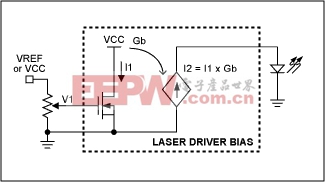 Figure 1b. |
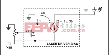 Figure 1c. | |
Figure 1. Open-loop methods for control of laser-bias current include (a) low-side control (laser-cathode grounded) with a variable resistor, or (b) a potentiometer driving a high-impedance input, and (c) high-side control (laser anode grounded) with a negative supply.
Circuit configurations for control of the laser-modulation level (Figures 2a and 2b) are similar to those for control of the bias current. Amplitude modulation of the data carrier produces a switched current. To increase the peak-to-peak amplitude of emitted light, lower the variable resistance in Figure 2a or increase V3 in Figure 2b. (These diagrams show the injection of bias current into the laser as well as modulation current.) In Figure 1b and 2b, note that the input stage of the laser driver IC, which carries I1 or I3, can be a bipolar npn transistor.
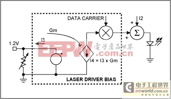 Figure 2a. | 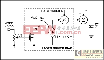 Figure 2b. |
模拟电路 模拟芯片 德州仪器 放大器 ADI 模拟电子 相关文章:
- 12位串行A/D转换器MAX187的应用(10-06)
- AGC中频放大器设计(下)(10-07)
- 低功耗、3V工作电压、精度0.05% 的A/D变换器(10-09)
- PIC16C5X单片机睡眠状态的键唤醒方法(11-16)
- 用简化方法对高可用性系统中的电源进行数字化管理(10-02)
- 利用GM6801实现智能快速充电器设计(11-20)