一种用于射频和微波测试系统的GaAsSb双异质结双极晶体管集
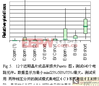
所有晶片工艺环节都由具有自动处理晶片功能的设备完成,以最大限度的减小人为因素造成的片与片、批与批之间的差异。具体的工艺步骤需要不断调整输入参数(例如,每一次要根据测试得到的目标层厚度进行离线计算),数据被不断收集以使统计工艺控制软件进行编程来指导操作者操作。
V.可靠性
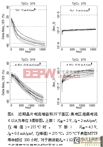
可靠性通过对分立的自对准1 × 3 μm2 HBTs进行高温寿命测试(HTOL)来确定,电流增益(??漂移是主要的可靠性失效模式。利用测试得到的激活能Ea, 其值大约为1.02 eV, 外推得到Tj = 125 °C.温度下MTTFs 寿命超过106 小时。电流增益(???漂移和基区?集电区电流泄漏(位列第二的主要可靠性失效模式)示于图?。以电流增益??漂移???作为失效标准同样示于图?,这一标准保证了??值始终保持在??以上。图?的下半部显示双异质结双极晶体管结构(例如,InP集电区)可在VCE = 4.5 V 下保持高可靠性工作,这一电压值比InP衬底单异质结双极晶体管高出 2 3 V。 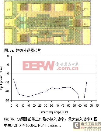
VI.电路性能
A.2 60 GHz 一比二静态分频器
静态分频器性能和芯片照片示于图7。双极晶体管HBT 用作静电放电保护。 其输入灵敏度窗口非常宽,单端正弦波输入状态下一比二除法功能可在2GHz到60GHz范围内实现。输入和输出可采用差分和单端方式。90 mA时偏置电压为-3.4V。典型输出功率从低频时的. 0 dBm 到高频60GHz时的 3 dBm 。
B.差分限幅放大器
由50个晶体管组成的差分限幅放大器照片示于图8a。限幅放大器采用两级Cherry-Hooper,一级cascode和一对有几级发射极跟随器缓冲的差分输出结构,低频小信号差分增益大于32dB, 单端(S-E)输入电压窗口为± 700 mV 最大单端(S-E)输出幅度500 mVpp 。 放大器从+1 V 到 4.1 V电源消耗0.59 W功率。偏置端采用 双极晶体管HBT 进行静电放电保护。输入输出均有差分失调/直流监测以及common-mode pull-up 能力.
图8b 显示了典型的在片增益特性,低频S-E 增益26.8±0.5 dB , 3 dB 带宽46.8±0.4 GHz.。达到65 GHz时群
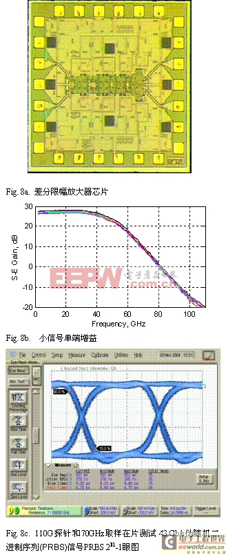
延时变化小于5 ps。典型 43 Gb/s 眼图输出信号如图8c 所示,其幅度为0.50 Vpp S E, 10%-90% 上升时间为9.2 ps, 总 RMS抖动378 fs。 295 fs RMS 抖动1 Vpp 差分PRBS 231-1 NRZ输入信号由以同样技术制作的半速retimer 提供。
C.线性相位检测器
这一电路在文献[18]中单独有详细介绍。它使用了超过200个最小尺寸的晶体管,并以HBT作为静电放电保护,3级互联,高值和低值电阻,电容,背面通孔。对于这样的复杂电路其在线成品率是合乎预期的。
ACKNOWLEDGMENT
We would like to thank Sue Harris and Denise Davis for technical RD assistance, and the Tech Center operations and engineering team for their manufacturing support.
REFERENCES
[1]T.S. Low, C.P. Hutchinson, P.C. Canfield, T.S. Shirley, R.E. Yeats, J.S.C. Chang, et al., “Migration from an AlGaAs to an InGaP emitter HBT IC process for improved reliability,” in Proc. GaAs IC Symposium 1998, pp. 153-156, 1998.
[2]B. Yeats, P. Chandler, M. Culver, D. D’Avanzo, G. Essilfie, C. Hutchinson, et al., “Reliability of InGaP-emitter HBTs,” in Proc. GaAs Mantech 2000, pp. 131-135, 2000.
[3]C.R. Bolognesi, N. Matine, M.W. Dvorak, X.G. Xu, J. Hu, and S. P. Watkins, “Non-blocking collector InP/GaAsSb /InP double heterojunction bipolar transistors with a staggered lineup base–collector junction,” IEEE Electron Device Lett., vol. 20, no. 4, pp. 155-157, 1999.
[4]M. Huffman, T. Engel, N. Pfister, G. Arevalo, T. Brown, M. Farhoud, et a l., “Dry etching of deep backside vias in InP,” in Proc. GaAs Mantech, pp.269-272, 2003.
[5]G. He, J. Howard, M. Le, P. Partyka, B. Li, G. Kim, et al., “Self-aligned InP DHBT with fT and fmax over 300 GHz in a new manufacturable technology,” IEEE Electron Device Lett., vol. 25, no. 8, pp. 520-522, 2004.
[6]S. Tsunashima, K. Murata, M. Ida, K. Kurishima, T. Kosugi, T. Enoki, et al., “A 150-GHz dynamic frequency divider using InP/InGaAs DHBTs,” in Proc. GaAs IC Symposium 2003, pp. 284-287, 2003.
[7]J. Godin, A. Konczykowska, M. Riet, P. Berdaguer, J. Moulu, V. Puyal, et al., “InP DHBT mixed-signal specific ICs for advanced 40 Gb/s transmitters,” in Proc. CSICS 2004, pp. 89-92, 2004.
[8]D.A. Hitko, T. Hussain, J.F. Jensen, Y. Royter, S.L. Morton, D.S. Matthews, et al., “A low power (45mW/latch) static 150GHz CML divider”, in Proc. CSICS 2004, pp. 167-170, 2004.
[9]R. E. Makon, K. Schneider, R. Driad, M. Lang, R. Aidam, R. Quay, and Q. Weimann, “Fundamental low phase noise InP-based DHBT VCOs with high output power operating up to 75 GHz”, in Proc. CSICS 2004, pp. 167-170, 2004.
[10]D. Sawdai, E. Kaneshiro, A. Gutierrez-Aitken, P.C. Grossman, K. Sato, et al., “High performance, high yield InP DHBT production process for 40 Gbps applications,” in Proc. IPRM 2001, pp. 493-496, 2001.
[11]Z. Griffith, M. Dahlstrom, M.J.W. Rodwell, X.-M. Fang, D. Lubyshev, Y. Wu, et al., “InGaAs-InP DHBTs for increased digital IC bandwidth having a 391-GHz fT and 505-GHz fmax,” IEEE Electron Device Lett., vol. 26, no. 1, pp. 11-13, 2005
[12]M. Urteaga, R. Pierson, P. Rowell, B. Brar, Z. Griffith, M. Dahlstrom, et al., “Wide bandwidth InP DHBT technology utilizing dielectric sidewall spacers,” in Proc. IPRM 2004, pp. 667-670, 2004.
[13]M.W. Dvorak, C.R. Bolognesi, O.J. Pitts, and S.P. Watkins, “300 GHz InP/GaAsSb/InP double HBTs with high current capability and BVceo ≥ 6V,” IEEE Electron Device Lett., vol. 22, no. 8, pp. 361-363, 2001.
[14]B.F. Chu-Kung and M. Feng, “InP/GaAsSb type-II DHBTs with fT > 350 GHz,” Electron. Lett., vol. 40, no. 20, pp. 1305-1306, 2004.
[15]X. Zhu, J. Wang, and D. Pavlidis, “First demonstration of low-power monolithic transimpedance amplifier using InP/GaAsSb/InP DHBTs,” in Proc. MTT-2005, Paper TU1D-6, 2005.
[16]A. Konczykowska, M. Riet, P. Berdaguer, P. Bove, M. Kahn, and J. Godin, “40 Gbit/s digital IC fabricated using InP/GaAsSb/InP DHBT technology,” Electronics Lett., vol. 41, no. 16, pp. 123-123, 2005.
[17]E.M. Cherry and D.E. Hooper, “The design of wide-band transistor feedback amplifiers,” Inst. Elec. Eng. Proc., vol. 110, no. 2, pp. 375-389, 1963
[18]R. Karlquist, C. Hutchinson, T. Marshall, and R. Van Tuyl, “A frequency agile 40 Gb/s half rate linear phase detector for data jitter measurement,” in Proc. CSICS 2005, to be published.
模拟电路 模拟芯片 德州仪器 放大器 ADI 模拟电子 相关文章:
- 12位串行A/D转换器MAX187的应用(10-06)
- AGC中频放大器设计(下)(10-07)
- 低功耗、3V工作电压、精度0.05% 的A/D变换器(10-09)
- PIC16C5X单片机睡眠状态的键唤醒方法(11-16)
- 用简化方法对高可用性系统中的电源进行数字化管理(10-02)
- 利用GM6801实现智能快速充电器设计(11-20)