关键参数的数模转换器多载波GSM / EDGE的发射机
时间:04-20
来源:互联网
点击:
Introduction
Emerging wireless communications standards (wide-band, multi-carrier) demand increasingly lower distortion and noise specifications.The digital-to-analog converters (DACs) in the transmitter (Tx) circuits are the key components for analog signal generation. They can significantly influence the system's ultimate dynamic performance.The transmitter sections of multi-carrier base station transceiver systems for GSM/EDGE present a chanllenge to communication DAC manufacturers. Manufacturers need to supply higher resolution and faster update rates, at higher output frequencies, all while reducing noise and spurious emissions over a wide bandwidth.
As a result of these requirements, GSM/EDGE system designers consider communications DACs attractive only if they can meet key specifications in four major noise and distortion categories. These are: Spurious-free Dynamic Range (SFDR), Signal-to-Noise Ratio (SNR), Intermodulation Distortion (IMD), and Multi-tone power ratio (MTPR). All four parameters are critical in ensuring that the Tx system meets required spurious and IMD targets.
DAC Dynamic Performance Requirements for GSM/EDGE
To specify noise and spurious emissions from base stations, a so-called GSM/EDGE Tx mask is used to identify the DAC requirements for these parameters. This mask shows that the allowable levels for noise and spurious emissions are dependent on the offset frequency from the transmitted carrier frequency. The GSM/EDGE mask and its specifications are based on a single active carrier with any other carriers in the transmitter being disabled. Specifications displayed in Figure 1 support per-carrier output power levels of 20W or greater. Lower output power levels will yield less stringent emission requirements.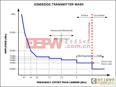
Figure 1. The Tx mask helps to identify the noise and distortion limits for DACs, used in the transmission path of a GSM/EDGE-based Base Station Transceiver System.
Spurious-free Dynamic Range (SFDR)
GSM/EDGE systems require the analog signal synthesis circuit block (the DAC) to have spurious emission levels of less than -80dBc for offset frequencies ≥ 6MHz. Spurious products from the DAC can combine with both random noise and spurious products from other circuit elements. The spurious products from the DAC should therefore be backed off a further 6dB (minimum) to allow for these other sources.The number of carriers and their signal levels with respect to the full-scale of the DAC also play an important role. Unlike a full-scale sine wave, the inherent nature of a multi-tone signal, in which the spectral energy of the signal is spread over a defined bandwidth, contains higher peak-to-rms ratios, raising the prospect for potential clipping, if the signal level hasn't been backed off appropriately. If a transmitter operates with four in-band carriers, each individual carrier must be operated at >12dB below full-scale while eight carriers require an amplitude of >18dB below full-scale to preclude waveform clipping.
Example: An EDGE-based modulation has a peak-to-rms ratio of 4dB for the 8-PSK (Phase-Shift Keying) modulation employed. This requires the carrier amplitude to be backed-off by another 4dB. An additional margin of -6dB is used to compensate for other circuit elements. For systems with four/eight carriers per designated bandwidth, each individual carrier must satisfy an amplitude specification of -18dBFS/-24dBFS or less.
Signal-to-Noise Ratio (SNR)
The SNR requirements for a GSM/EDGE-based system can again be derived from the GSM/EDGE Tx mask (Figure 1). With a worst-case noise level of -80dBc at frequency offsets of ≥ 6MHz and an assumed measurement bandwidth of 100kHz, the minimum noise density per Hertz is calculated as follows:SNRMIN = -80dB - 10 × log10(100 × 103Hz)Since random DAC noise will add to both the spurious tones and to random noise from other circuit elements, it is recommended to reduce the specification limits by about 10dB to allow for these additional noise contributions while maintaining compliance with the GSM/EDGE mask values.
SNRMIN = -130dB/Hz >
模拟电路 模拟芯片 德州仪器 放大器 ADI 模拟电子 相关文章:
- 12位串行A/D转换器MAX187的应用(10-06)
- AGC中频放大器设计(下)(10-07)
- 低功耗、3V工作电压、精度0.05% 的A/D变换器(10-09)
- PIC16C5X单片机睡眠状态的键唤醒方法(11-16)
- 用简化方法对高可用性系统中的电源进行数字化管理(10-02)
- 利用GM6801实现智能快速充电器设计(11-20)