基于MAX8784设计的TFT-LCD电源技术
本文介绍了MAX8784主要特性,方框图,典型工作电路图和所用元件列表,MAX8784评估板主要特性,电路图和评估板元件列表。
Maxim 公司的MAX8784是TV和监视器的TFT-LCD电源解决方案,包括升压稳压器,调整的正和负电荷泵,三个大电流运输放大器,以及双模式逻辑控制高压开关控制区块。输入电压4V-5.5V。效率高达90%,开关频率1.2MHz,主要用在LCD TV和LCD 监视器。
MAX8784主要特性:
_ Step-Up Regulator Supply for LCD Panel Source Driver
Fast Transient Response to Pulsed Load
Built-In 18V, 4A, 0.11??n-Channel Power MOSFET with Lossless Current Sensing
Cycle-by-Cycle Current-Limit Comparator 90% Efficiency (5V In to 15V Out)
1.2MHz Switching Frequency
_ Three High-Current 19V Operational Amplifiers
180mA Output Short-Circuit Current
45V/μs Slew Rate
20MHz Bandwidth
Rail-to-Rail Input and Output Operation
_ Regulated Charge-Pump Tripler with Integrated Diodes for TFT Gate-On Supply
_ Regulated Charge Pump for TFT Gate-Off Supply
_ Built-In Sequencing Internal Digital Soft-Start
36V Gate-On Switch
Startup Timing Capacitors for AVDD and GON
_ Undervoltage and Thermal Protection
_ 4V to 5.5V Input Operating Range
MAX8784应用:
LCD TVs and LCD Monitors
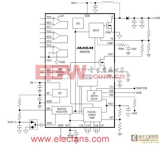
图1。MAX8784功能方框图
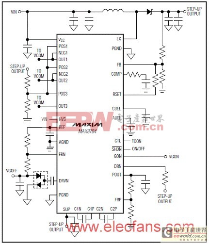
图2。MAX8784简化工作电路图
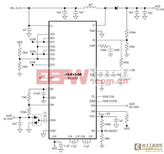
图3。MAX8784典型工作电路图
工作电路元件列表:

图4。MAX8784 HVS模式工作电路图
MAX8784评估板
The MAX8784 evaluation kit (EV kit) is a fully assembled and tested surface-mount PCB that provides the voltages and features required for active-matrix, thin-film transistor (TFT) liquid-crystal display (LCD) panels in LCD monitors and LCD TVs. The EV kit contains a stepup switching regulator, a two-stage positive charge pump for the TFT gate-on supply, a single-stage negative charge pump for the TFT gate-off supply, and three high-current op amps. Two capacitor-control delays are available: one to control the initial startup of the stepup, and the other to control the delay between the negative and positive charge pumps. Also included is a logic-controlled, high-voltage switch for the positivegate driver supply. A high-voltage stress (HVS) mode is provided to increase the step-up and the positive charge-pump output voltages for stress testing the display panel during production. A capacitive dummy load is provided at the high-voltage switch output for ease of testing without a panel attached.
The EV kit operates from a DC supply voltage of +4.5V to +5.5V, as configured. The step-up switching regulator is configured for a +14V output providing at least 700mA. The positive charge pump is configured for a +28V output providing at least 50mA. The negative charge pump is configured for a -9V output providing at least 50mA. The three high-current op amps are each configured for a +7V output that can source or sink 180mA. The high-voltage switch can be controlled by external logic. The EV kit’s input voltage range can be lowered to +4V at slightly lower load currents.
The MAX8784 step-up switching regulator operates at 1.2MHz, allowing the use of tiny surface-mount components.
The MAX8784 thin QFN package (0.8mm max height), with low-profile external components, allows this circuit to be less than 3mm high.
MAX8784评估板主要特性:
? +4.5V to +5.5V Input-Voltage Range
? Output Voltages
+14V Output at 700mA (Step-Up Switching Regulator)
+28V Output at 50mA (Positive Charge Pump)
-9V Output at 50mA (Negative Charge Pump)
Three High-Current Op Amps (±180mA)
? 1.2MHz Switching Frequency
? All Output Voltages are Resistor Adjustable
? Logic-Controlled, High-Voltage Switch
? High-Voltage Stress Mode for the Step-Up and
Positive Charge-Pump Output Voltages
? Capacitor-Controlled Initial Startup Delay and Positive Charge-Pump Delay
? Low-Profile Surface-Mount Components
? Fully Assembled and Tested
图5。MAX8784评估板电路图
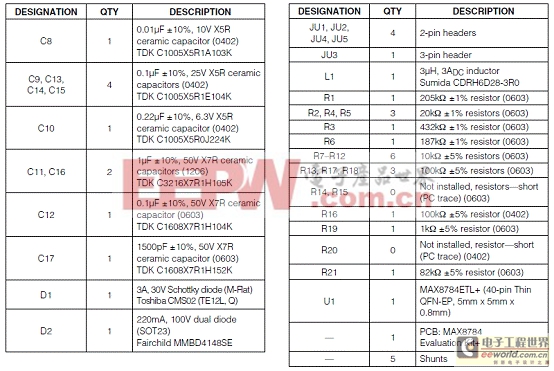
MAX8784评估板元件列表:

模拟电源 电源管理 模拟器件 模拟电子 模拟 模拟电路 模拟芯片 德州仪器 放大器 ADI 相关文章:
- 采用数字电源还是模拟电源?(01-17)
- 模拟电源管理与数字电源管理(02-05)
- 数字电源正在超越模拟电源(03-19)
- 数字电源PK模拟电源(04-03)
- TI工程师现身说法:采用数字电源还是模拟电源?(10-10)
- 开关电源与模拟电源的分别(05-08)
