Simple Methods Reduce Input Ri
| Q = C.V | , where I = 800mA, T = 3600s (1Hr), and V = 3.4V. | |
| I.T = C.V |
Thus, C = 847 farads and fFILTER = 0.12mHz. The sum of ESR and battery contact resistance (about 100mΩ) limits the attenuation to a maximum of 21dB, assuming the ripple source resistance (RFILTER) equals 1Ω. The model for an actual battery is more complex, with the central bulk capacitance modified by ESR, ESL, and parasitic capacitance. In practice one should add capacitance close to RFILTER, thereby providing high frequency assistance and low ESR above 250kHz ( 50mΩ) to the battery and its interconnect leads. A typical value for the additional CFILTER is 470nF. For the MAX665 circuit of Figure 10, increasing CFILTER to 1500μF lowers the input voltage and current ripple as shown in Figure 11.
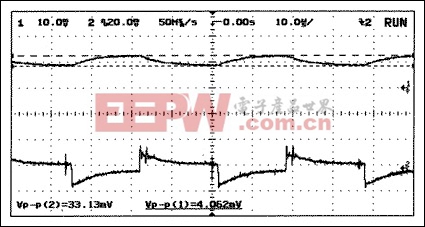
Figure 10. Input Voltage and Current Ripple for the RC-filter circuit (Figure 9): CIN = CFILTER = 100μF, and RFILTER = 2.2Ω. Charge pump is a MAX665. Input current ripple (upper trace): 100mA/div. Input voltage ripple (lower trace): 20mV/div, AC coupled.
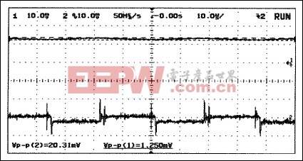
Figure 11. Input voltage and current ripple for the RC-filter circuit of Figure 7, with 1500μF quasi-battery capacitor: CIN =100μF, CFILTER = 1500μF, RFILTER = 2.2Ω, and MAX665 charge pump. Input current ripple (upper trace): 100mA/div. Input voltage ripple (lower trace): 20mA/div, AC coupled.
Conclusion
Several methods are available for reducing the effect of input power-supply ripple caused by charge pumps. Placing an LC filter in addition to the input capacitor recommended by the data sheet, for instance, (#2) provides excellent voltage-ripple protection to the rest of the system (Figure 10) with minimal effect on the overall conversion efficiency. An effective alternative for battery systems is a simple series resistor (#4), which occupies minimal space. The resistor is also suitable in non-battery applications for which large storage values (> 50μF) are appropriate. Results of a simulated battery application are shown in Figure 11.
An overview of Maxim's charge-pump ICs (Table 1) is included to help the reader choose an appropriate device according to the desired clock frequency, mode of operation, and level of output current required.
Table 1 Product Selection
| Package | 8-SO | 16-wSO | 8-μMax/SO | 8-μMax/SO |
| I/P Volts | 1.5V to 5.5V | 1.5V to 8V | 1.5V (inv) or 2.5V to 5.5V | 1.5V (inv) or 2.5V to 5.5V |
| O/P Current | 100mA | 100mA | 50mA | 50mA |
| Pump Rate | 10kHz/80kHz | 10kHz/45kHz | 3kHz/50kHz/130kHz | 13kHz/100kHz/250kHz |
| Mode | -VIN, +2VIN | -VIN, +2VIN | -VIN, +2VIN | -VIN, +2VIN |
| Regulated | No | No | No | No |
| Package | 8-SO | 8-SO | 5-SOT23 | 5-SOT23 |
| I/P Volts | 2.0V to 5.5V | 2.0V to 8V | 1.5V (inv) or 2.5V to 5.5V | 1.5V (inv) or 2.5V to 5.5V |
| O/P Current | 125mA | 125mA | 45mA | 45mA |
| Clock Freq | 125kHz/250kHz | 500kHz/1MHz | 12kHz | 35kHz |
| Mode | -VIN, +2VIN | -VIN, +2VIN | +2VIN | +2VIN |
| Regulated | No | No | No | No |
| Package | 5-SOT23 | 5-SOT23 | 6-SOT23 | 6-SOT23 |
| I/P Volts | 1.4V to 5.5V | 1.4V to 5.5V | 1.5V to 5.5V | 1.5V to 5.5V |
| O/P Current | 25mA | 25mA | 60mA | 25mA |
| Clock Freq | 125kHz | 500kHz | 12kHz/35kHz/125kHz/250kHz | 12kHz |
| Mode | -VIN | -VIN | -VIN | -VIN |
| Regulated | No | No | No | No |
| Package | 6-SOT23 | 16-QSOP | 8-μMax | 8-SO |
| I/P Volts | 1.5V to 5.5V | 2.0V to 6.0V | 1.5V to 6.0V | 2.0V to 6.0V |
| O/P Current | 25mA | ±10mA | ±10mA | ±10mA |
| Clock Freq | 125kHz | 7kHz/33kHz/100kHz/185kHz | 24kHz | 8kHz |
| Mode | -VIN | +2VIN and -VIN | +2VIN and -VIN | +2VIN and -VIN |
| Regulated | No | No | No | No |
| Package | 8-μMax | 8-SO | 8-μMax | 8-SO |
| I/P Volts | 2.0V to 3.6V | 4.5V to 5.5V | 1.8V to 3.6V | 2.7V to 5.5V |
| O/P Current | 60mA | 30mA | 20mA | 250mA |
| Clock Freq | 500kHz | 500kHz | 330kHz/1MHz | 200kHz/1MHz |
| Regulated | Yes | Yes | Yes | Yes |
| Package | 8-μMax | 8-μMax | 16-QSOP | 8-SO |
模拟电源 电源管理 模拟器件 模拟电子 模拟 模拟电路 模拟芯片 德州仪器 放大器 ADI 相关文章:
- 采用数字电源还是模拟电源?(01-17)
- 模拟电源管理与数字电源管理(02-05)
- 数字电源正在超越模拟电源(03-19)
- 数字电源PK模拟电源(04-03)
- TI工程师现身说法:采用数字电源还是模拟电源?(10-10)
- 开关电源与模拟电源的分别(05-08)