建设电源工程
时间:05-29
来源:互联网
点击:
Component Placement
When laying out the PCB for this example, you should first place the DC-DC converter IC (MAX1742), the inductor, and the input and output capacitors. Then, move those components so the input capacitor is close to the MAX1742's input pins, the inductor is close to the IC's LX pin, and the output capacitor is close to the inductor and the IC's ground pins. Seldom are all these criteria compatible with one another, and often one of the component locations must be compromised to optimize another.The most critical node in most cases is the common ground between the input and output capacitors and the ground pin of the IC. These three grounds must be very close, usually within 10mm of one another (Figure 2a-2b). During the charge cycle (Figure 2a), current flows from the input capacitor through the high-side switch, through the inductor, through the output capacitor, across the ground plane, and back into the input capacitor. During the discharge cycle (Figure 2b) current continues to flow through the inductor, through the output capacitor, across the ground plane, back through the IC's ground pin, through the low-side switch, and back into the inductor.
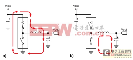
Figure 2. These diagrams illustrate current paths during the charge (a) and discharge (b) cycles.
Because this circulating current can interfere with other circuits, its path length must be kept short. (Short paths also contribute to stable operation and good efficiency.) Too long a path length in the ground portion (during either cycle) can compromise the 0V reference for other circuit elements. That condition can also lead to poor regulation, excessive output ripple, and even loss of function. Placing the input capacitor ground, output capacitor ground, and IC ground adjacent to each other minimizes those unwanted effects.
The next most important connection, the junction between the inductor and the output capacitor, keeps the regulator's output impedance low. The remaining two connections are of equal sensitivity, and one or the other may be somewhat compromised; either by longer traces to circumnavigate other PCB elements, or by vias in the conductor path.
Power Ground
After placing components according to the criteria above, the common ground is connected, either with wide traces or with a polygon of solid copper. Use as much copper as possible to create a low-impedance path between the elements.Local Ground
The typical application circuit for many DC-DC converter ICs indicates multiple symbols for ground, which is an excellent hint on how to accomplish a successful circuit layout. One of the different symbols often indicates a local ground plane. Elements that connect to the local ground plane can include reference-bypass capacitors, resistor dividers, and resistors that set operating points (such as resistor RTOFF in the example).The local ground plane is also a solid copper polygon, usually connected to the power ground plane at one point only; typically the pin titled PGND. Local ground planes prevent switching currents from polluting the low-noise local ground plane. Such currents often exceed 10A.
Ground Plane
Because many systems rely on a separate ground plane for all components on the PCB, it is often tempting to use the ground plane of the DC-DC converter section for that purpose. Such an option should be avoided in all cases. The switching currents mentioned above can cause catastrophic ground glitches across the board, producing excessive EMI, causing invalid logic states, and raising the noise floor. The proper interface between DC-DC converter circuitry and the ground plane is a single via (or a small grouping of multiple vias), leading from the poured copper power ground to the buried ground plane.Signal Routing
After completing the initial ground layout, make the required connections for the first four critical components and then place and route the remaining components. A useful approach is to take all non-critical signals to the backside of the PCB with small vias, reserving the top side of the board for the routing of critical traces.Many approaches are available for signal routing on circuit boards. An easy way is to consider the DC and AC components of a signal, and route accordingly. Remember that every wire is a resistor and an inductor as well. Each signal must be considered with regard to its use in the circuit to determine optimal trace width and length. High-speed and high-current signals demand short, wide routing traces. Longer, thinner traces are appropriate for non-critical signals such as low-speed logic.
Verification
After the converter is completed, the boards manufactured, and the components assembled, the overall design should be verified for performance to the original criteria. If the design was implemented diligently with regard to the issues discussed above, the chances for initial success are good. But, even the best power supply designers must often tweak their designs, and sometimes repeat the whole process when they uncover new issues or ones previously unconsidered.Efficiency
Efficiency can be a key performance parameter. That is usually the case for devices operating from a battery, and is especially true for power supplies in laptop computers. Power supply efficiency in laptop computers affects battery life, but it also contributes power dissipation, and it should be coordinated with the heat-removal limitations. Note that a converter supplying 50W at 85% efficiency dissipates 7.5W inside the computer case.In laptops, the efficiency is important over a wide range of operating conditions. Examples include low battery, full battery, and battery charging, under both standby and operating states. In other applications, the efficiency-critical points depend on how the device is used. Light-load efficiency and quiescent operating current are most important in a pager, while full-load efficiency and heat generation are most critical in network hardware.
Load Regulation
A converter's ability to stay within the specified output-voltage tolerance regardless of load is called load regulation. It applies at DC, but it also includes fast transients such as those encountered with Intel Speed-Step? processors. You should verify that the output voltage stays within specification when loaded with currents ranging from zero to the maximum. Ensure that the output voltage does not undershoot its minimum value when the load changes quickly from minimum to maximum, and also ensure that the output voltage does not exceed its maximum value when the load current goes from maximum to minimum.Line Regulation
The converter's ability to maintain output-voltage regulation with a varying input voltage is called line regulation. Again, it should be examined both at DC and with a fast AC transient. An AC transient is encountered when a laptop computer switches from its wall supply to it internal battery, and when it switches back from battery to the wall supply. In some systems, the voltage change can be as large as 10V. Verify that the output voltage stays within specification when the input voltage changes from minimum to maximum, and make sure that step changes in the input voltage do not cause peaks or valleys in the output voltage that exceed the output-voltage specifications.Temperature Sensitivity
Often, a system is evaluated in a lab setup and then deemed ready for prime time. But, a critical condition that needs further examination is operation over the worst-case operating-temperature range. Performance to the electrical criteria above should be recorded for comparison at the highest and lowest temperatures the system will encounter during operation. Watch for parameters that change drastically, and those that approach upper or lower limits over temperature.The best way to evaluate a system over temperature is to use an environmental chamber. The chamber lets you conduct computer-controlled experiments over a broad range of temperature, and with an accuracy of 1°C or better. Because most people don't have a chamber handy, however, they must make do with less sophisticated equipment. Common heat guns and even hairdryers are useful in heating a circuit while under test. To cool a circuit well below ambient temperature, spray it with a compressed inert gas called cold spray (offered in many technical catalogs).
Conclusion
Power supply design is neither rocket science nor common knowledge. It is something that is learned, and usually the hard way. But, applying the principles in this article can eliminate some of the missteps while putting you on the road to becoming a successful power-supply designer.模拟电源 电源管理 模拟器件 模拟电子 模拟 模拟电路 模拟芯片 德州仪器 放大器 ADI 相关文章:
- 采用数字电源还是模拟电源?(01-17)
- 模拟电源管理与数字电源管理(02-05)
- 数字电源正在超越模拟电源(03-19)
- 数字电源PK模拟电源(04-03)
- TI工程师现身说法:采用数字电源还是模拟电源?(10-10)
- 开关电源与模拟电源的分别(05-08)