Crystal Considerations with Da
时间:12-28
来源:互联网
点击:
- the system power off.
- Wait for a period of time (two hours, 24 hours, etc.). The longer the time period, the easier it is to measure the accuracy of the clock.
- Turn the system on again, read clock, and compare to the known accurate clock.
- Resynchronize the RTC to the known accurate clock.
- Keep the system powered up and wait for a period of time equal to the period in Step 3.
- Read the clock after waiting for the above period of time and compare it to the known accurate clock.
Since it is possible for noise to be coupled onto the crystal pins, care must be taken when placing the external crystal on a PC board layout. It is very important to follow a few basic layout guidelines concerning the placement of the crystal on the PC board layout to ensure the extra clock ticks do not couple onto the crystal pins.
- It is important to place the crystal as close as possible to the X1 and X2 pins. Keeping the trace lengths between the crystal and RTC as small as possible reduces the probability of noise coupling by reducing the length of the antenna. Keeping the trace lengths small also decreases the amount of stray capacitance.
- Keep the crystal bond pads and trace width to the X1 and X2 pins as small as possible. The larger these bond pads and traces are, the more likely it is that noise can couple from adjacent signals.
- If possible, place a guard ring (connected to ground) around the crystal. This helps isolate the crystal from noise coupled from adjacent signals. See Figure 2 for an illustration of using a guard ring around a crystal.
- Try to ensure that no signals on other PC board layers run directly below the crystal or below the traces to the X1 and X2 pins. The more the crystal is isolated from other signals on the board, the less likely it is that noise is coupled into the crystal. There should be a minimum of 0.200 inches between any digital signal and any trace connected to X1 or X2. The RTC should be isolated from any component that generates electromagnetic radiation (EMR). This is true for discrete and module type RTCs.
- It may also be helpful to place a local ground plane on the PC board layer immediately below the crystal. This helps to isolate the crystal from noise coupling from signals on other PC board layers. Note that the ground plane needs to be in the vicinity of the crystal only and not on the entire board. See Figure 5 for an illustration of a local ground plane. Note that the perimeter of the ground plane does not need to be larger than the outer perimeter of the guard ring.
C = εA/t, where
ε = dielectric constant of the PC board
A = area of the traces/pads
t = thickness of the PC board layer
Therefore, to determine if a ground plane is appropriate for a given design, the above parameters must be taken into account to ensure that the capacitance from the local ground plane is not sufficiently large enough to slow down the clock.
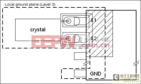
Figure 5. Recommended layout for crystal.
Checking For Oscillation
The first impulse that a designer has when checking for oscillator operation often is to connect an oscilloscope probe to the oscillator input (X1) or output (X2) pin. Doing so is not recommended when using a Real-Time Clock. Since the oscillator is designed to run at low power (which extends operating time from a battery), loading the oscillator with an oscilloscope probe is likely to stop the oscillator. If the oscillator does not stop, the additional loading will reduce the signal amplitude, and may cause erratic operation, such as varying amplitude. Oscillation should therefore be verified indirectly.Oscillation can be verified several ways. One method is to read the seconds register multiple times, looking for the data to increment. On RTCs with an OSF (Oscillator Stop Flag), clearing and then monitoring this bit will verify that the oscillator has started and is continuously running. These methods won't work if the designer is troubleshooting a design and cannot communicate with the RTC. An alternate method is to check the square wave output on RTCs that have a square wave output. Check the datasheet to verify if the RTC must be written first to enable the oscillator and square wave output. Note that most RTC square wave outputs are open-drain, and require a pull up resistor for operation. The square wave output can also be used to verify the accuracy of the RTC, however, a frequency counter with sufficient accuracy must be used.
Fast Clocks
The following are the most common scenarios that cause a crystal-based RTC to run fast.模拟电路 模拟芯片 德州仪器 放大器 ADI 模拟电子 相关文章:
- 12位串行A/D转换器MAX187的应用(10-06)
- AGC中频放大器设计(下)(10-07)
- 低功耗、3V工作电压、精度0.05% 的A/D变换器(10-09)
- PIC16C5X单片机睡眠状态的键唤醒方法(11-16)
- 用简化方法对高可用性系统中的电源进行数字化管理(10-02)
- 利用GM6801实现智能快速充电器设计(11-20)