SLIC电源设计-SLIC Power-Supply Des
时间:01-30
来源:互联网
点击:
Abstract: Integrated communication systems incorporate voice service with data service. Such systems use subscriber-line interface card (SLIC) functions to maintain compatibility with legacy equipment. The voltages required in these systems vary from country to country and depends on the particular application. This article discusses how to derive various voltages required in such systems using the MAX668 boost controller. Split feedback to improve cross-regulation is presented. An example of an isolated power supply is also presented.
Subscriber-line interface cards (SLICs) provide the interface between the telephone-service provider and the telephone handset in your home. They operate in two main modes: On-hook refers to when the handset is idle and waiting for a signal indicating that someone wants to make a connection, and off-hook refers to when the handset is active and the user is trying to complete a connection. Telephone-system voltages are traditionally negative to prevent electromigration from eroding the installed copper wiring.
Telephone systems require certain special voltages that vary from application to application and country to country. This article presents circuits for deriving these voltages from commonly available supply voltages. Table 1 summarizes the input and output characteristics of the circuits.
Table 1. Inputs and Outputs
The on-hook voltage, which generates the ringer voltage, is typically -72V in the United States and as high as -150V in other countries. The ringer voltage, a 20Hz to 60Hz sinusoid, drives an electromechanical bell in the handset that can be located far from the central office (CO). The off-hook voltage is typically -48V in the United States, although some localized systems use -24V. This voltage powers the system during voice communications. The CO provides power for the telephone system independently from the electric utility, allowing the telephone to work during a power outage.
With advances in data-communication technology, companies are incorporating voice service with data service to provide integrated communication systems. Such systems require SLIC functions to maintain compatibility with legacy equipment. The following circuits demonstrate techniques for generating SLIC voltages from commonly available voltages. All of the circuits are based on a transformer flyback topology using a MAX668 boost controller. This topology achieves compact magnetics and flexible output voltages.

Figure 1. This simple transformer flyback inverter gene rates -48V from a +5V input.
Q1 is selected to switch 9A peak current with VGS = 3.8V (4.5 VIN-VBE). A snubber for the flyback voltage is not necessary, because the breakdown voltage of Q1 is nine times' the voltage reflected back from the secondary to primary transformer winding. R7 and C7 filter the current-sense signal to prevent false triggering caused by switching noise. The moderate switching frequency (165kHz) allows good efficiency with parts of moderate cost and performance.
The transformer (T1) is wound on a Coiltronics SG4 gapped core with AL = 75nH/T2. The primary winding is eight turns of #22AWG, so the primary inductance is 4.8μH. The secondary winding is 64 turns of #28AWG, making the turns ratio 1:8. The switch duty cycle is approximately 55%, which gives close to the optimal power transfer for a given magnetic volume.
A lower-cost fast-recovery diode (D1) is used instead of a Schottky diode, because the lower switching frequency minimizes the impact of the reverse-recovery time on the switching efficiency. Also, the high-output voltage minimizes the advantage of a lower forward-voltage diode. Because the output voltage is negative, the feedback must be inverted by an op amp (U2) to match the switching controller (U1). D2 protects the inverting input from being pulled negative. R3 and C5 provide the dominant pole for feedback-loop stability.
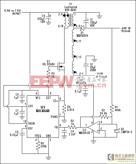
Figure 2. The transformer flyback topology allows the on-hook (-100V) and off-hook (-24V) voltages to be generated using a single controller by adding an extra secondary winding.
The transformer (T1) is an off-the-shelf unit from Coiltronics that allows fast circuit development. A custom transformer can be designed and optimized for volume production. The primary inductance is 3.8μH, and the turns ratio is 1:1:3. This makes the duty cycle approximately 80% instead of 50% for optimal power transfer. The result is higher peak current compared with an optimized transformer.
The -24V output is fed back through the op-amp inverter (U2), regulating the output to ±1% directly. The -100V output uses the transformer-turns ratio for regulation. This works as long as the power output from the -100V supply is not significantly more than the power output from the fed-back voltage. The typical application does not require tight regulation of the -100V on-hook voltage, and so ±10% is sufficient.

Figure 3. The transformer flyback topology can be optimized for power transfer by choosing the transformer-turns ratio such that the switching regulator operates at a 50% duty cycle.

Figure 4. Splitting the feedback between the on-hook and off-hook voltages allows moderate regulation of both outputs.
The transformer is a custom design for this application. The leakage inductance, which represents the imperfect coupling between the primary and secondary windings, is large enough to require snubbing of the primary flyback voltage to prevent breakdown of the switching transistor. R8 and C8 slow down the switch transition and dissipate some of the energy in the leakage inductance to limit the maximum flyback voltage. The Coiltronics Versa-Pac line of transformers is tri-filar wound for maximum coupling (meaning, three wires are wound in parallel), so leakage inductance is minimized. The trade-off is decreased flexibility in the turns ratio and lower isolation-voltage rating between the primary and secondary windings.

Figure 5. Electrical isolation between the input and the output is implemented by taking advantage of the inherent isolation provided by the transformer and adding isolation for the feedback voltage.
The isolated feedback from the -24V output is implemented with a shunt regulator and an optoisolator. The shunt regulator combines a voltage reference and an error amplifier to generate a current-error signal. The error current drives the photodiode in the optoisolator, which modulates and isolates the current in the phototransistor.
The optoisolator is selected for a nominally 100% current-transfer ratio at 10mA. The error current is converted to an error voltage through R4. R4 and C13 create a pole in the loop response that limits the loop bandwidth to 2.8kHz. The loop compensation must take into account the signal delay of the optoisolator as well as the additional gain of the shunt regulator combined with the error amp in the MAX668.
A similar version of this article appeared in the February 20, 2001 issue of TechOnLine magazine.
Subscriber-line interface cards (SLICs) provide the interface between the telephone-service provider and the telephone handset in your home. They operate in two main modes: On-hook refers to when the handset is idle and waiting for a signal indicating that someone wants to make a connection, and off-hook refers to when the handset is active and the user is trying to complete a connection. Telephone-system voltages are traditionally negative to prevent electromigration from eroding the installed copper wiring.
Telephone systems require certain special voltages that vary from application to application and country to country. This article presents circuits for deriving these voltages from commonly available supply voltages. Table 1 summarizes the input and output characteristics of the circuits.
Table 1. Inputs and Outputs
Figure 1 | ||||
Figure 2 | ||||
Figure 3 | ||||
Figure 4 | ||||
Figure 5 |
The on-hook voltage, which generates the ringer voltage, is typically -72V in the United States and as high as -150V in other countries. The ringer voltage, a 20Hz to 60Hz sinusoid, drives an electromechanical bell in the handset that can be located far from the central office (CO). The off-hook voltage is typically -48V in the United States, although some localized systems use -24V. This voltage powers the system during voice communications. The CO provides power for the telephone system independently from the electric utility, allowing the telephone to work during a power outage.
With advances in data-communication technology, companies are incorporating voice service with data service to provide integrated communication systems. Such systems require SLIC functions to maintain compatibility with legacy equipment. The following circuits demonstrate techniques for generating SLIC voltages from commonly available voltages. All of the circuits are based on a transformer flyback topology using a MAX668 boost controller. This topology achieves compact magnetics and flexible output voltages.
-48V Output from +5V Supply
The circuit in Figure 1 generates -48V at 300mA for customer premises equipment (CPE) or client-side equipment from a +4.5V minimum input. The input voltage also is the gate-drive voltage for the MAX668 (U1), limiting the input voltage to +5.5V (maximum). The MOSFET switch (Q1) presents more gate capacitance than the controller can drive efficiently; therefore, complementary emitter followers (Q2, Q3) buffer the gate-drive output.Figure 1. This simple transformer flyback inverter gene rates -48V from a +5V input.
Q1 is selected to switch 9A peak current with VGS = 3.8V (4.5 VIN-VBE). A snubber for the flyback voltage is not necessary, because the breakdown voltage of Q1 is nine times' the voltage reflected back from the secondary to primary transformer winding. R7 and C7 filter the current-sense signal to prevent false triggering caused by switching noise. The moderate switching frequency (165kHz) allows good efficiency with parts of moderate cost and performance.
The transformer (T1) is wound on a Coiltronics SG4 gapped core with AL = 75nH/T2. The primary winding is eight turns of #22AWG, so the primary inductance is 4.8μH. The secondary winding is 64 turns of #28AWG, making the turns ratio 1:8. The switch duty cycle is approximately 55%, which gives close to the optimal power transfer for a given magnetic volume.
A lower-cost fast-recovery diode (D1) is used instead of a Schottky diode, because the lower switching frequency minimizes the impact of the reverse-recovery time on the switching efficiency. Also, the high-output voltage minimizes the advantage of a lower forward-voltage diode. Because the output voltage is negative, the feedback must be inverted by an op amp (U2) to match the switching controller (U1). D2 protects the inverting input from being pulled negative. R3 and C5 provide the dominant pole for feedback-loop stability.
-24V and -100V Output from +5.5V Supply
The circuit in Figure 2 generates -24V at 150mA and -100V at 50mA for CPE from a +5.5V minimum input provided by a wall adapter. The MAX668 (U1) has an internal linear regulator that generates a +5V rail for the gate-drive voltage. The MOSFET (Q1) is selected to switch 7A peak current with VGS = 4.5V. Snubbing the flyback voltage is not necessary, because the leakage inductance is low and the breakdown voltage of Q1 is more than two times' the reflected output voltage. R5 in series with the gate of Q1 slows down the turn-on time to minimize the switching noise seen by the current-sense amp.Figure 2. The transformer flyback topology allows the on-hook (-100V) and off-hook (-24V) voltages to be generated using a single controller by adding an extra secondary winding.
The transformer (T1) is an off-the-shelf unit from Coiltronics that allows fast circuit development. A custom transformer can be designed and optimized for volume production. The primary inductance is 3.8μH, and the turns ratio is 1:1:3. This makes the duty cycle approximately 80% instead of 50% for optimal power transfer. The result is higher peak current compared with an optimized transformer.
The -24V output is fed back through the op-amp inverter (U2), regulating the output to ±1% directly. The -100V output uses the transformer-turns ratio for regulation. This works as long as the power output from the -100V supply is not significantly more than the power output from the fed-back voltage. The typical application does not require tight regulation of the -100V on-hook voltage, and so ±10% is sufficient.
-24V and -48V Output from +12V Supply
The circuit in Figure 3 generates -24V at 50mA and -48V at 100mA from a +12V nominal input. It demonstrates the optimal turns ratio for power transfer in the transformer. The primary to -24V secondary turn ratio is 1:2, and the primary to -48V secondary turns ratio is 1:4. Therefore, the switching regulator operates at 50% duty cycle. The -48V output is fed back to the controller for regulation. The -24V output is regulated to ±5% by the turns ratio and close coupling of the secondary windings.Figure 3. The transformer flyback topology can be optimized for power transfer by choosing the transformer-turns ratio such that the switching regulator operates at a 50% duty cycle.
-24V and -72V Output with Split Feedback from +12V Supply
The circuit in Figure 4 generates -24V at 400mA and -72V at 100mA from a +12V nominal input. Both outputs are regulated to ±5% under all combinations of line and load by splitting the feedback between the two outputs. The trade-off is to give up a little tolerance on the off-hook voltage for tighter tolerance on the on-hook voltage. The feedback ratios are based on the relative output powers. The -24V output delivers 4/7 of the maximum output power; thus, the feedback resistor is scaled to supply 4/7 of the current required for regulation. Similarly, the -72V output delivers 3/7 of the maximum output power, so the feedback resistor supplies 3/7 of the current required for regulation.Figure 4. Splitting the feedback between the on-hook and off-hook voltages allows moderate regulation of both outputs.
The transformer is a custom design for this application. The leakage inductance, which represents the imperfect coupling between the primary and secondary windings, is large enough to require snubbing of the primary flyback voltage to prevent breakdown of the switching transistor. R8 and C8 slow down the switch transition and dissipate some of the energy in the leakage inductance to limit the maximum flyback voltage. The Coiltronics Versa-Pac line of transformers is tri-filar wound for maximum coupling (meaning, three wires are wound in parallel), so leakage inductance is minimized. The trade-off is decreased flexibility in the turns ratio and lower isolation-voltage rating between the primary and secondary windings.
Isolated +3.3V, -24V, and -72V Output from +5V Supply
The circuit in Figure 5 generates isolated +3.3V at 100mA, -24V at 100mA, and -72V at 25mA from a nominal +5V input. Isolation is required when the input voltage is not isolated from the line (either electric utility or telephone system power). The transformer isolates the +5V input from the output voltages. The +3.3V output is generated from an extra secondary winding. A linear post-regulator is required because of the wide voltage ratio between +3.3V and -24V used for feedback. The -72V output regulation is not critical and relies on the turns ratio and close coupling to the -24V secondary winding.Figure 5. Electrical isolation between the input and the output is implemented by taking advantage of the inherent isolation provided by the transformer and adding isolation for the feedback voltage.
The isolated feedback from the -24V output is implemented with a shunt regulator and an optoisolator. The shunt regulator combines a voltage reference and an error amplifier to generate a current-error signal. The error current drives the photodiode in the optoisolator, which modulates and isolates the current in the phototransistor.
The optoisolator is selected for a nominally 100% current-transfer ratio at 10mA. The error current is converted to an error voltage through R4. R4 and C13 create a pole in the loop response that limits the loop bandwidth to 2.8kHz. The loop compensation must take into account the signal delay of the optoisolator as well as the additional gain of the shunt regulator combined with the error amp in the MAX668.
A similar version of this article appeared in the February 20, 2001 issue of TechOnLine magazine.
SLIC 电源设 Power-Supply 相关文章:
- 实话实说电源设计(01-22)
- 通用电源设计指南(05-22)
- 具有多个电压轨的FPGA和DSP电源设计实例(05-22)
- 具有多个电压轨的FPGA和DSP电源设计实例(二) (05-22)
- 电源设计小贴士3:开关电源阻尼输入滤波器(02-03)
- 一种适合教学的开关电源设计及调试(09-06)