什么是JESD204?我们为何要关注它?
时间:08-02
来源:互联网
点击:
JESD204 – Why Should We Pay Attention to It?
In much the same way as LVDS began overtaking CMOS as the technology of choice for the converter digital interface several years ago, JESD204 is poised to tread a similar path in the next few years. While CMOS technology is still hanging around today, it is mostly been overtaken by LVDS. The speed and resolution of converters as well as the desire for lower power eventually renders CMOS and LVDS inadequate for converters. As the data rate increases on the CMOS outputs, the transient currents also increase and result in higher power consumption. While the current, and thus power consumption, remains relatively flat for LVDS, the interface has an upper speed bound that it can support. This is due to the driver architecture as well as the numerous data lines that must all be synchronized to a data clock. Figure 4 illustrates the different power consumption requirements of CMOS, LVDS, and CML outputs for a dual 14-bit ADC.

Figure 4. CMOS, LVDS, and CML Driver Power Comparison
At approximately 150 – 200 MSPS and 14 bits of resolution, CML output drivers start to become more efficient in terms of power consumption. CML offers the advantage of requiring fewer output pairs per a given resolution than LVDS and CMOS drivers due to the serialization of the data. The CML drivers specified for the JESD204B interface have an additional advantage since the specification calls for reduced peak to peak voltage levels as the sample rate increases and pushes up the output line rate. The number of pins required for the same give converter resolution and sample rate is also considerably less. Table 1 gives an illustration of the pin counts for the three different interfaces using a 200 MSPS converter with various channel counts and bit resolutions. The data assumes a synchronization clock for each channel’s data in the case of the CMOS and LVDS outputs and a maximum data rate of 4.0 Gbps for JESD204B data transfer using the CML outputs. The reasons for the progression to JESD204B using CML drivers become obvious when looking at this table and observing the dramatic reduction in pin count that can be achieved.
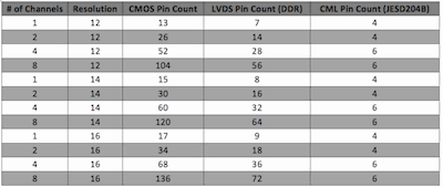
Table 1. Pin Count Comparison – 200 MSPS ADC (click on figure for PDF of the table)
We have seen the trend that is pushing the converter digital interface towards the JESD204 interface defined by JEDEC. Our company has been involved with the standard from the beginning when the first JESD204 specification was released. To date, Analog Devices has released to production several converters with the JESD204 and JESD204A compatible outputs and is currently developing products with outputs that are compatible with JESD204B.
Summary
As the speed and resolution of converters have increased, the demand for a more efficient digital interface has increased as well. The industry began realizing this with the JESD204 serialized data interface. The interface specification has continued to evolve to offer a better and faster way to transmit data between converters and FPGAs (or ASICs). The interface has undergone two revisions to improve upon its implementation and meet the increasing demands brought on by higher speeds and higher resolution converters. Looking to the future of converter digital interfaces, it is clear that JESD204 is poised to become the industry choice for the digital interface to converters. Each revision has answered the demands for improvements on its implementation and has allowed the standard to evolve to meet new requirements brought on by changes in converter technology. As system designs become more complex and converter performance pushes higher, the JESD204 standard should be able to adapt and evolve to continue to meet the new design requirements necessary.
In much the same way as LVDS began overtaking CMOS as the technology of choice for the converter digital interface several years ago, JESD204 is poised to tread a similar path in the next few years. While CMOS technology is still hanging around today, it is mostly been overtaken by LVDS. The speed and resolution of converters as well as the desire for lower power eventually renders CMOS and LVDS inadequate for converters. As the data rate increases on the CMOS outputs, the transient currents also increase and result in higher power consumption. While the current, and thus power consumption, remains relatively flat for LVDS, the interface has an upper speed bound that it can support. This is due to the driver architecture as well as the numerous data lines that must all be synchronized to a data clock. Figure 4 illustrates the different power consumption requirements of CMOS, LVDS, and CML outputs for a dual 14-bit ADC.
Figure 4. CMOS, LVDS, and CML Driver Power Comparison
At approximately 150 – 200 MSPS and 14 bits of resolution, CML output drivers start to become more efficient in terms of power consumption. CML offers the advantage of requiring fewer output pairs per a given resolution than LVDS and CMOS drivers due to the serialization of the data. The CML drivers specified for the JESD204B interface have an additional advantage since the specification calls for reduced peak to peak voltage levels as the sample rate increases and pushes up the output line rate. The number of pins required for the same give converter resolution and sample rate is also considerably less. Table 1 gives an illustration of the pin counts for the three different interfaces using a 200 MSPS converter with various channel counts and bit resolutions. The data assumes a synchronization clock for each channel’s data in the case of the CMOS and LVDS outputs and a maximum data rate of 4.0 Gbps for JESD204B data transfer using the CML outputs. The reasons for the progression to JESD204B using CML drivers become obvious when looking at this table and observing the dramatic reduction in pin count that can be achieved.
Table 1. Pin Count Comparison – 200 MSPS ADC (click on figure for PDF of the table)
We have seen the trend that is pushing the converter digital interface towards the JESD204 interface defined by JEDEC. Our company has been involved with the standard from the beginning when the first JESD204 specification was released. To date, Analog Devices has released to production several converters with the JESD204 and JESD204A compatible outputs and is currently developing products with outputs that are compatible with JESD204B.
Summary
As the speed and resolution of converters have increased, the demand for a more efficient digital interface has increased as well. The industry began realizing this with the JESD204 serialized data interface. The interface specification has continued to evolve to offer a better and faster way to transmit data between converters and FPGAs (or ASICs). The interface has undergone two revisions to improve upon its implementation and meet the increasing demands brought on by higher speeds and higher resolution converters. Looking to the future of converter digital interfaces, it is clear that JESD204 is poised to become the industry choice for the digital interface to converters. Each revision has answered the demands for improvements on its implementation and has allowed the standard to evolve to meet new requirements brought on by changes in converter technology. As system designs become more complex and converter performance pushes higher, the JESD204 standard should be able to adapt and evolve to continue to meet the new design requirements necessary.
- SoC面临挑战,智能分割顺势而起(11-07)
- PC电源常见故障判断分析与排除 (04-16)
- UWB定位,新一代的精确定位技术(09-20)
- 本土单芯片射频收发器帮助减少TD-SCDMA商用障碍 (11-20)
- TD-SCDMA技术获突破,首颗CMOS单芯片射频芯片完成流片(01-06)
- USB 2.0高速端口的ESD保护(07-28)